

Semiconductor Equipment Primer - $1.3 Trillion of Market Cap Monopoly and One Problem Nobody Wants to Talk About
The most comprehensive semiconductor equipment analysis on the internet, and the three things consensus is getting wrong.


“Gradually, then suddenly.”
Ernest Hemingway, The Sun Also Rises, on how bankruptcy happens. Also, apparently, how consensus trades form.
Semiconductor equipment is the most crowded “smart money” trade in global equities right now, and almost nobody holding it has modeled the single biggest risk correctly.
Eighteen months ago, these stocks were orphans. Applied Materials traded at 13x forward earnings. ASMi was left for dead. The market had decided that semiconductor equipment companies were cyclical industrials with China exposure, not AI beneficiaries, and rotated every available dollar into Nvidia and the hyperscalers. If you mentioned ASML at a dinner party in early 2025, someone would nod politely and change the subject to Mag Seven positioning.
Then the stocks doubled.
TSMC raised capex to $56 billion. Memory pricing exploded. Order books filled for two years out. The buy-side collectively discovered that every AI chip in existence must be physically manufactured, that physical manufacturing requires machines, and that five companies in the Netherlands, California, and Japan hold a monopoly on those machines. The “picks and shovels” analogy went from niche observation to consensus gospel in about six months. NTM P/E multiples expanded from 13 to 22x at the trough to 29 to 40x today. Analyst notes that used to say “cyclical headwinds” now say “structural AI beneficiary.” The narrative machine did what it always does: it showed up late and declared victory.
We are not here to tell you that semiconductor equipment companies are great businesses. You already know that. The stocks already reflect it. If you are reading this hoping for 10,000 words confirming that ASML has a monopoly and TSMC’s capex is going up, save yourself the time.
We are here to tell you three things the consensus is getting wrong.
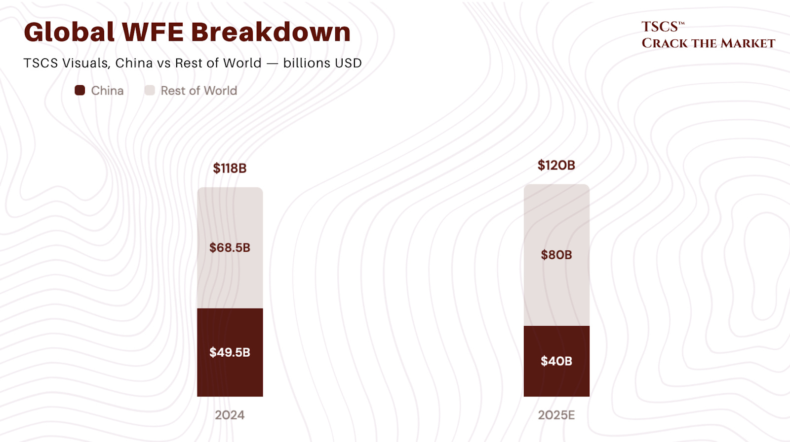
First, peak China is behind us, and the revenue hole is larger than most models assume. China represented 42% of global WFE spending in 2024, roughly $49.5 billion. That number was not organic demand. It was panic stockpiling ahead of export controls, state-directed capacity buildout, and a pre-buy surge led by Huawei (which went from zero WFE spending in 2022 to $7.3 billion in 2024, becoming the fourth-largest equipment customer globally). The gap between trend spending ($30 to 35 billion) and actual 2024 spending implies $10 to 15 billion of pull-forward that will not repeat. Every major Western semicap company is now guiding for materially lower China revenue. Meanwhile, Chinese domestic equipment makers are growing 35 to 50% annually and have captured an estimated 35% of their home market, beating Beijing’s own interim targets. The question is not whether domestic substitution happens. It is how fast.
Second, the “9% WFE CAGR” consensus is probably right on the headline number and almost certainly wrong on the composition. The mix is shifting permanently: away from mature-node tools (where Chinese substitution is fastest) toward leading-edge logic and advanced packaging (where Western monopolies are unassailable). Investors pricing semicap stocks on a blended growth rate without adjusting for the mix shift are, in our view, making a mistake. KLA’s process control franchise and ASML’s EUV monopoly are not the same business as Tokyo Electron’s mature-node etch tools selling into Chinese fabs, yet the market prices all of them on the same WFE growth assumption.
Third, the structural bull case is actually stronger than the consensus version, but for different reasons than most people cite. The real story is not “AI demand is big” (it is, but that is priced). The real story is that every major technology transition happening simultaneously (Gate-All-Around transistors, backside power delivery, 3D stacking, HBM scaling) is a step-function increase in equipment intensity per dollar of semiconductor output. Tool reuse rates are collapsing at the 2nm node. TSMC is processing both sides of the wafer for the first time. Wafer stacking is going from 7% to 35%+ of total consumption by 2030. The equipment companies are not just riding a demand wave. They are benefiting from a permanent increase in the ratio of equipment spending to chip output. That is a fundamentally different (and more durable) growth driver than “hyperscalers are spending a lot.”
This piece is our attempt to build the analysis that captures all three of those dynamics in one place, rather than pretending the first risk does not exist while cheerleading the third.
What this post is
This is a joint analysis between TSCS and Ozeco. His work forms the technical and structural backbone: the most detailed semiconductor equipment primer we have encountered outside of institutional sell-side coverage.
What TSCS has layered on top is an investment framework, editorial opinions throughout, and a comprehensive analysis of the China risk that most semicap primers either ignore entirely or dismiss in a single paragraph.
Together, we cover:
What semiconductors are and why the $800 billion chip market is heading to $1.5 trillion by 2030
The $1 trillion value chain from sand to electronics, and where the pricing power actually lives
How chips are built and the taxonomy of the $120 billion WFE market
TSMC, Foundry 2.0, and why the world’s most important company is simultaneously a monopoly and a single point of failure
The semicap oligopoly: who does what, why consolidation is frozen, and who owns which chokepoints
WFE growth drivers for the next decade: AI capex, reshoring, the memory supercycle, and why capital intensity math matters more than headline growth rates
China’s self-sufficiency mandate: why Western semicap has likely seen its best China quarters, where the moats are (and are not), and the vulnerability spectrum from most to least exposed
TSMC pushing Moore’s Law further: GAA, backside power delivery, and the technology roadmap through the 2030s
The back-end revolution: advanced packaging, CoWoS, 3D stacking, and why testing and bonding are the new AI bottleneck
The investor playbook: company-by-company analysis with TSCS opinions on positioning, relative value, and what we would actually own
Where we agree with Ozeco, we say so briefly. Where we disagree, we say so loudly. Where the consensus is wrong, we say that loudest of all.
This is not a primer for beginners, although beginners will learn an enormous amount. This is a primer for investors who want to understand the sector well enough to have a differentiated view. There is a difference, and it is roughly the distance between reading a sell-side initiation and actually knowing where to put your money.
A note on Ozeco
I want to say something about my collaborator, because it matters for context.
I first came across Ozeco’s work when we were building our first semiconductor coverage, specifically the Semiconductors - The Worlds Most Important Sector and our deep dives on Lam Research and Naura. What struck me was not just the depth (which is exceptional) but the granularity of the supply chain mapping.
Most semiconductor analysis, even at the institutional level, treats the equipment layer as a black box: “TSMC buys machines, machines are expensive, ASML has a monopoly.” Ozeco opens the black box and shows you every component, every market share figure, every technology transition, every customer relationship. The factual architecture of this piece is his.
He has done many great posts, some of them include:
“AI Investment Supercycle: How to Invest in the $3-4tn Race”
“TSMC: Manufacturing the World’s AI Compute”
“Optical & Networking SUpercycle at the Hear of the AI Revolution”
What TSCS adds is the “so what.” The investment opinions, the China risk framework, the company-level positioning calls, the uncomfortable questions that a pure primer does not ask. We think the combination works: his breadth with our edge.
If you care about semiconductors, read Ozeco. If you want to invest in them, read us both. I would strongly encourage you to subscribe to his publication.
Why you need to be reading TSCS
TSCS is institutional-grade equity research for investors who think for themselves. Over 4,500 subscribers spanning professional fund managers, family offices, and sophisticated individual investors who want analysis, not tips.
Recent work:


Free subscribers see our process. Premium subscribers see our positions.
Let’s get into it.
What are chips? The backbone of modern society
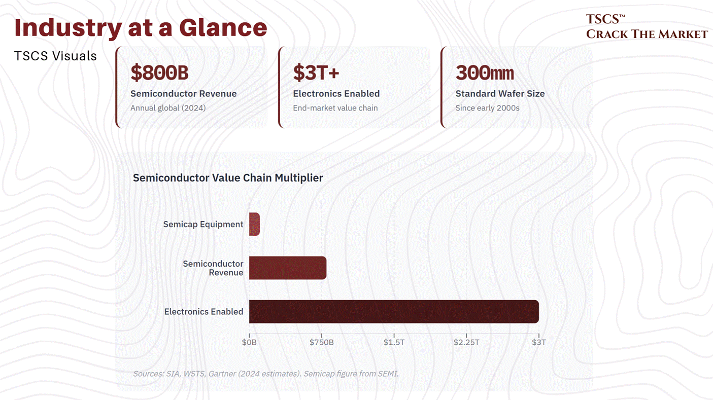
Everything you touch that requires electricity contains a semiconductor. Your phone. Your car. Your washing machine. The traffic lights on your commute. The power grid keeping the lights on while you read this. Semiconductors are not a “sector.” They are the substrate on which modern civilization operates, and the $800 billion they generate in annual revenue is a rounding error relative to the $3 trillion electronics value chain they enable.
A semiconductor (or integrated circuit) is, at its most reductive, a tiny black square of silicon with electronic circuits printed on it. Wafers of silicon are processed, circuits are etched into layers, and the wafer is then sliced into rectangular dies. Packages protect and connect those bare chips to the outside world. That is the 30-second version. The 30-year version is considerably more interesting, and considerably more expensive.
The wafer: where it all starts
Chips are made on wafers, circular slabs of ultra-pure silicon sliced from a crystal boule. When you see foundry capacity quoted in “wafers per month” (wpm), this is what they mean: how many finished wafers can roll off the production line.
Wafer size matters enormously. The industry standardized on 300mm diameter wafers in the early 2000s, and that is where it has stayed. Moving from 200mm to 300mm multiplied the usable surface area by 2.25x, meaning 2.25 times more chips per wafer. For two decades prior to 300mm, the industry rebased its entire cost structure every 15 years by enlarging the wafer. That game is over. 450mm wafers were expected around 2015 to 2017. They never arrived, and almost certainly never will.
Our view: This is an underappreciated point that most semiconductor primers gloss over. The death of wafer enlargement is one of the structural reasons why Moore’s Law economics have deteriorated. The industry lost its simplest lever for cost reduction, which means every subsequent gain in chip economics must come from shrinking transistors (increasingly expensive), stacking chips vertically (advanced packaging), or improving yields (process control). This is precisely why equipment companies like ASML, ASMi and KLA have such extraordinary pricing power today. The easy physics is exhausted. What remains is hard engineering, and hard engineering requires expensive machines.
A chip is a skyscraper, not a pancake
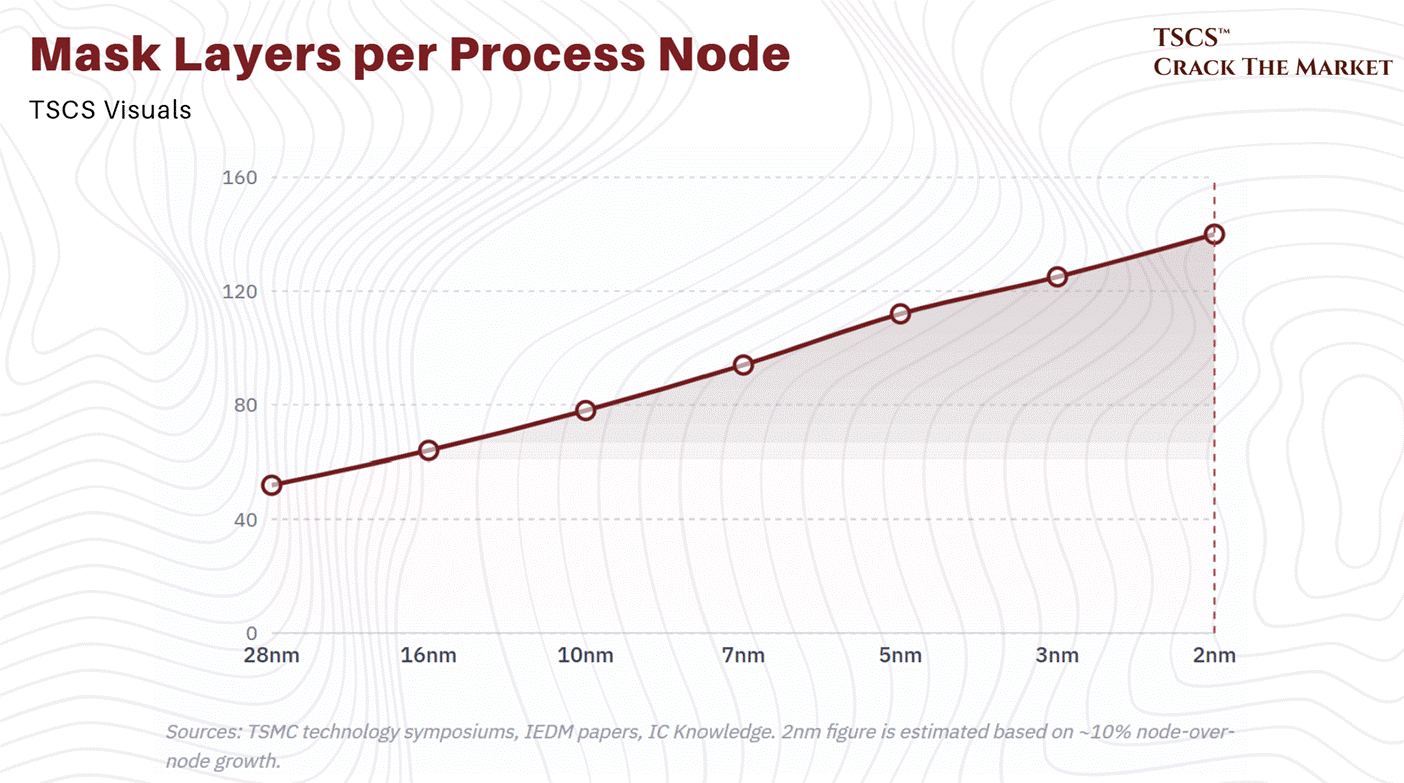
Most people imagine a chip as flat. It is not. A modern chip is a vertical stack of dozens, sometimes over a hundred, layers. At the bottom sits the substrate (silicon) where transistors, the elementary building blocks, are carved at dimensions measured in single-digit nanometers. The middle layers contain interconnections between transistors, wired with copper, cobalt, and tungsten. The top layers carry progressively larger features.
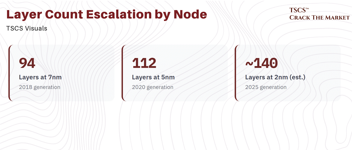
For every new manufacturing node, the number of layers increases by roughly 10%. A 7nm chip has 94 layers. A 5nm chip has 110 to 115. The trajectory is obvious and relentless: more layers, more complexity, more equipment required per wafer, more revenue per tool for the companies making the machines.
At the very bottom of this stack sits the transistor. Think of it as a switch, either on or off, 1 or 0. A single chip can contain billions of these switches. The most advanced semiconductors today contain upwards of $20 billion worth of R&D in their design alone. A chip is a Lego set with blocks measured in atoms.
Our view: The layer count escalation is one of those deceptively simple data points that tells you almost everything about the semicap investment case. Every additional layer means another pass through deposition, lithography, etch, and inspection equipment. A 10% increase in layers per node does not translate to a 10% increase in WFE demand (tool reuse, efficiency gains, and batch processing all matter), but it does translate to structurally rising equipment intensity per wafer. This is the compounding engine underneath the semicap growth story and it is remarkably difficult to disrupt, because the physics of making thinner, taller structures requires more precise tools, not fewer. As Ozeco details later in this piece, 2nm capacity expansion now costs $350m per 1,000 wafers per month versus $160m for 5nm. That is not inflation. That is physics.
The $1tn semiconductor value chain: From sand to electronics
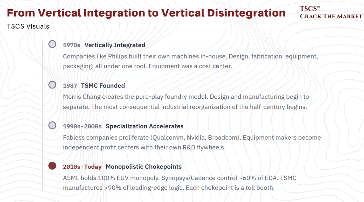
The semiconductor industry did not always look like this. In the 1970s, companies like Philips built their own machines in-house. Design, fabrication, equipment, packaging: all under one roof. That vertical integration is dead. What replaced it is one of the most elegant and ruthless supply chains in industrial history, a chain where every link is a chokepoint and every chokepoint is a toll booth.
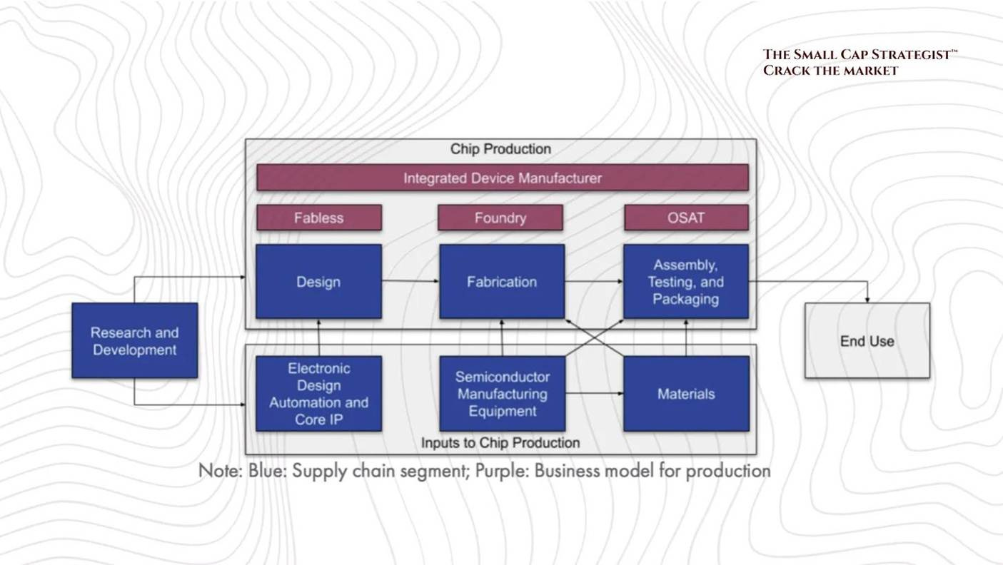
The value chain, from bottom to top:
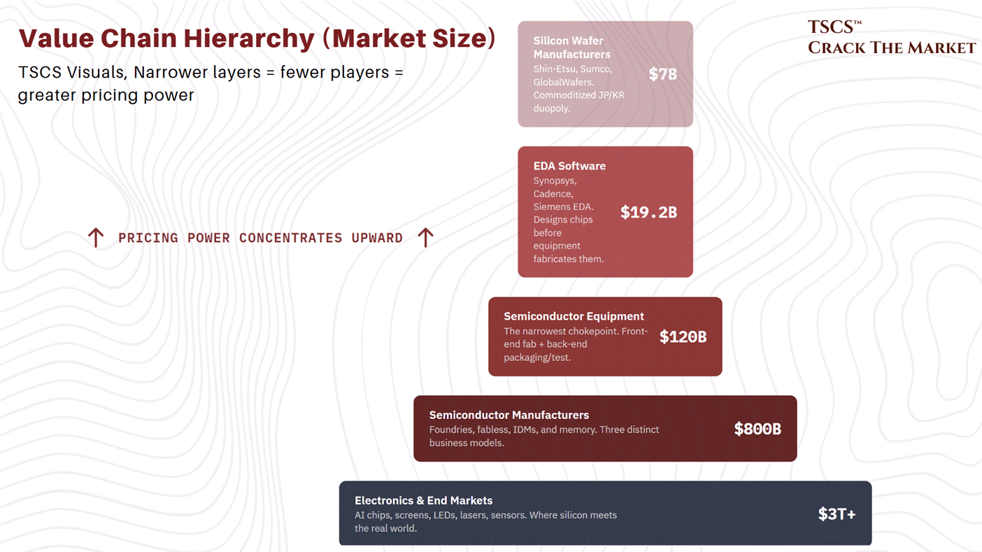
The chain begins with silicon wafer manufacturers ($7 billion market), companies like Shin-Etsu, Sumco, and GlobalWafers that slice ultra-pure semiconductor material into the substrates on which everything else is built. This is a Japanese and South Korean duopoly, largely commoditized, and not where the interesting economics live.
The interesting economics live one layer up: semiconductor equipment ($120 billion market). These are the companies that build the machines foundries like TSMC use to print circuits onto silicon. Front-end equipment handles the actual chip fabrication on wafers. Back-end equipment handles packaging and testing. The names that matter here (Applied Materials, ASML, Lam Research, Tokyo Electron, ASMi, KLA) will dominate the rest of this analysis, and for good reason. They sit at the narrowest point of the entire semiconductor funnel.
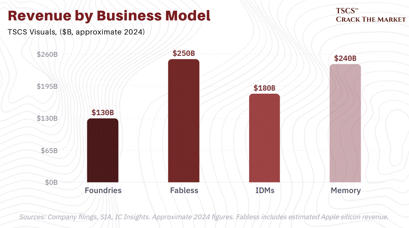
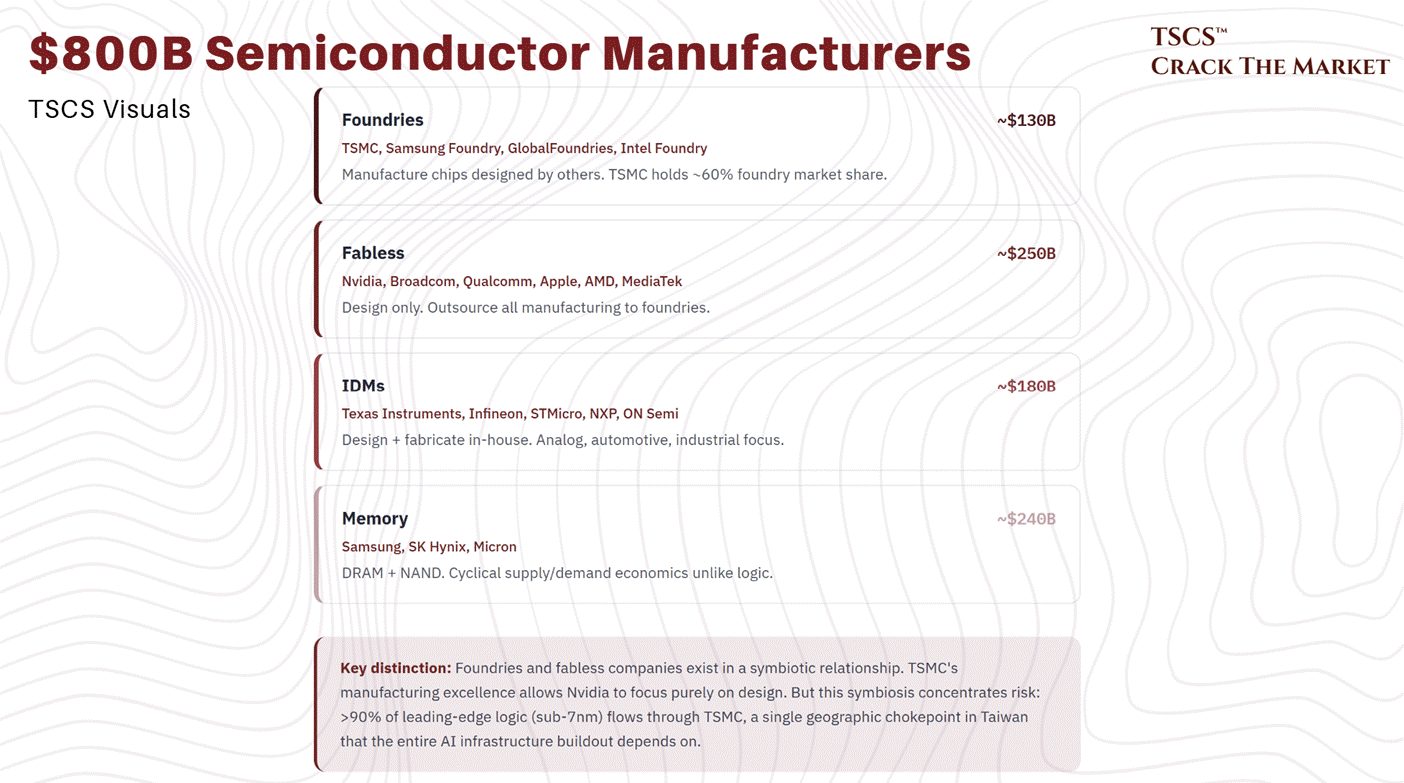
Below them sit the semiconductor manufacturers ($800 billion market), which break into three distinct business models. Foundries (TSMC, GlobalFoundries, Samsung’s foundry division, and Intel Foundry) specialize in manufacturing chips designed by other companies. Fabless companies (Nvidia, Broadcom, Qualcomm, Apple) do the designing. Integrated Device Manufacturers, or IDMs (Texas Instruments, Infineon, STMicroelectronics), handle everything from design through fabrication and testing in-house, typically focused on analog and mature-node chips for automotive and industrial applications. Memory sits in its own category (Samsung, SK Hynix, Micron), with economics driven by supply/demand cycles that look nothing like logic.
Adjacent to the equipment chain sits EDA software (Synopsys, Cadence, Siemens EDA), a market that generated $19.2 billion in revenue in 2024 according to the Electronic System Design Alliance, with Synopsys and Cadence each holding roughly 30% global share. EDA designs the chips before equipment fabricates them, and the relationship is directly causal: as EDA tools enable more sophisticated architectures (chiplets, 3D stacking, heterogeneous integration, backside power delivery), the equipment required to fabricate those designs becomes correspondingly more advanced and more expensive. Synopsys’s flows are already certified for TSMC’s A16 and N2P processes, including support for backside routing, meaning the design complexity that drives equipment intensity is being baked into chips years before they reach the fab floor.
At the bottom of the chain sits the $3 trillion electronics market. AI chips, screens, LEDs, lasers, sensors. This is where the silicon meets the real world.
Our view: The vertical disintegration of the semiconductor industry is one of the most consequential industrial reorganizations of the past half-century, and most investors still do not appreciate its implications for equipment companies. When Philips made its own tools, the equipment was a cost center. When TSMC buys from ASML, the equipment is a profit center for an independent monopolist with its own R&D flywheel. The disintegration created structural pricing power that did not exist in the integrated era. ASML does not negotiate prices the way a captive internal division would. It charges what the physics demands, because no one else can supply what it supplies. This dynamic, independent equipment monopolists selling into capacity-constrained foundries, is the core reason semicap margins have expanded for two decades and will likely continue expanding.
The three pillars of semiconductor products
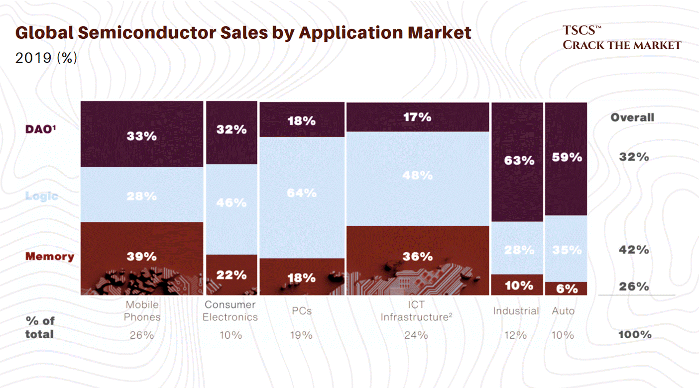
Semiconductors are not one market. They are three, each with distinct economics, customers, and cycle dynamics.
Logic (42% of industry revenues) contains the “brains” of computing. CPUs, GPUs, application processors, microcontrollers. This is where Nvidia, AMD, Intel, Apple, and Qualcomm compete. It is the segment most directly tied to the AI investment cycle, because every training run and every inference query requires logic silicon. Microcontrollers are the quieter cousin: small computers on a single chip embedded in cars, industrial automation, consumer appliances. Less glamorous, but ubiquitous.
Memory (26% of industry revenues) stores the data that logic processes. DRAM is volatile (loses data without power) and serves as the buffer between storage and processor. NAND is non-volatile (retains data without power) and provides permanent storage in SSDs, phones, and data centers. Memory is a brutally cyclical commodity business where pricing swings of 30 to 50% in a single year are normal. The current HBM (High Bandwidth Memory) supercycle has temporarily broken this pattern, but investors should not confuse a structural shift in one memory subsegment with a permanent repeal of memory cycle economics.
Our view: The HBM versus commodity memory distinction is worth quantifying. HBM pricing per bit runs at roughly 5-6x standard DRAM, and the manufacturing process requires 2-3x more equipment steps due to TSV (through-silicon via) drilling, wafer thinning, and hybrid bonding. The three producers (Samsung, SK Hynix, Micron) are capacity-constrained through 2026, which is why HBM pricing has remained firm. But standard DRAM and NAND remain commodity markets. CXMT is scaling to 280,000-300,000 wafers per month and targeting 10-12% global DRAM share by end 2025. YMTC is producing competitive 232-layer NAND despite being entity-listed. The structural bull case for HBM is real. Extrapolating it to “memory broadly” requires ignoring the supply side, and the supply side has historically been where memory bulls go to die.
Discrete, Analog, and Other (32% of revenues) covers the semiconductors that interface with the physical world: voltage regulators, data converters, power management ICs, RF chips, sensors. These translate continuous real-world signals (temperature, sound, pressure) into digital information and back again. Texas Instruments and Analog Devices dominate. The economics here are different from logic: longer product lifecycles, stickier customer relationships, lower peak growth but higher margin stability. This is the “boring but beautiful” corner of semiconductors.
Leading edge vs. mature nodes: two different industries sharing one name
This distinction matters enormously for understanding where equipment spending goes, and most generalist investors blur it.
Leading-edge nodes (currently 3nm, soon 2nm) are where Moore’s Law operates. The objective is miniaturization and performance: cramming as many transistors as possible onto increasingly smaller chips to maximize computing power per watt. This is AI territory. This is Apple’s latest iPhone processor. This is where ASML’s EUV machines are mandatory and where TSMC has an unassailable monopoly on manufacturing.
For a time, the consensus was that Moore’s Law was dead. The cost of transitioning from one node to the next kept rising, and investors rotated toward “More than Moore” plays like advanced packaging. That consensus was wrong. ASML demonstrated at its Capital Markets Day that AI is actually accelerating Moore’s Law: computing power for AI workloads is increasing 16x every two years, eight times faster than mainstream semiconductors. Energy consumption is rising 5x every two years versus 0.6x for everything else. The implication is clear: lithography (the process of printing ever-smaller features) is more important in the age of AI than it has ever been, because it is the primary mechanism for controlling both cost and energy consumption at scale.
Our view: The “Moore’s Law is dead” narrative was, in hindsight, one of the worst consensus calls in recent semiconductor history. It was dead for smartphones and PCs, where the marginal performance gain from a node shrink no longer justified the cost premium for most consumers. It was never dead for hyperscalers spending $600 billion annually on AI infrastructure who will pay any price for 25 to 30% better power efficiency. The AI capex supercycle did not revive Moore’s Law. It revealed that Moore’s Law had merely been waiting for a customer willing to pay for it. That customer arrived, and its name is compute-hungry AI. This is the single most important reframing for understanding semicap valuations today. We detail the specific transistor architecture transitions (FinFET to GAA to CFET) and their equipment implications in the technology section.
Mature nodes (28nm and above) serve a completely different market. Automotive, industrial, power management, RF. Innovation here comes not from shrinking transistors but from novel materials (silicon carbide, gallium nitride) and increased customization. These chips only use DUV lithography (no EUV required), which means ASML’s older tool lines, Nikon, and Canon all compete. The growth story is electrification and digitalization: more chips per vehicle, more chips per factory, more chips per kilowatt of renewable energy infrastructure.
The $800 billion market heading to $1.2 to 1.5 trillion by 2030
The semiconductor market is projected to grow from $800 billion today to over $1 trillion by 2026 and $1.25 trillion by 2028, driven by data centers, automotive, and industrial applications. The dominant growth engine is servers, data centers, and storage, estimated at a 14% CAGR versus 9% for the overall market.
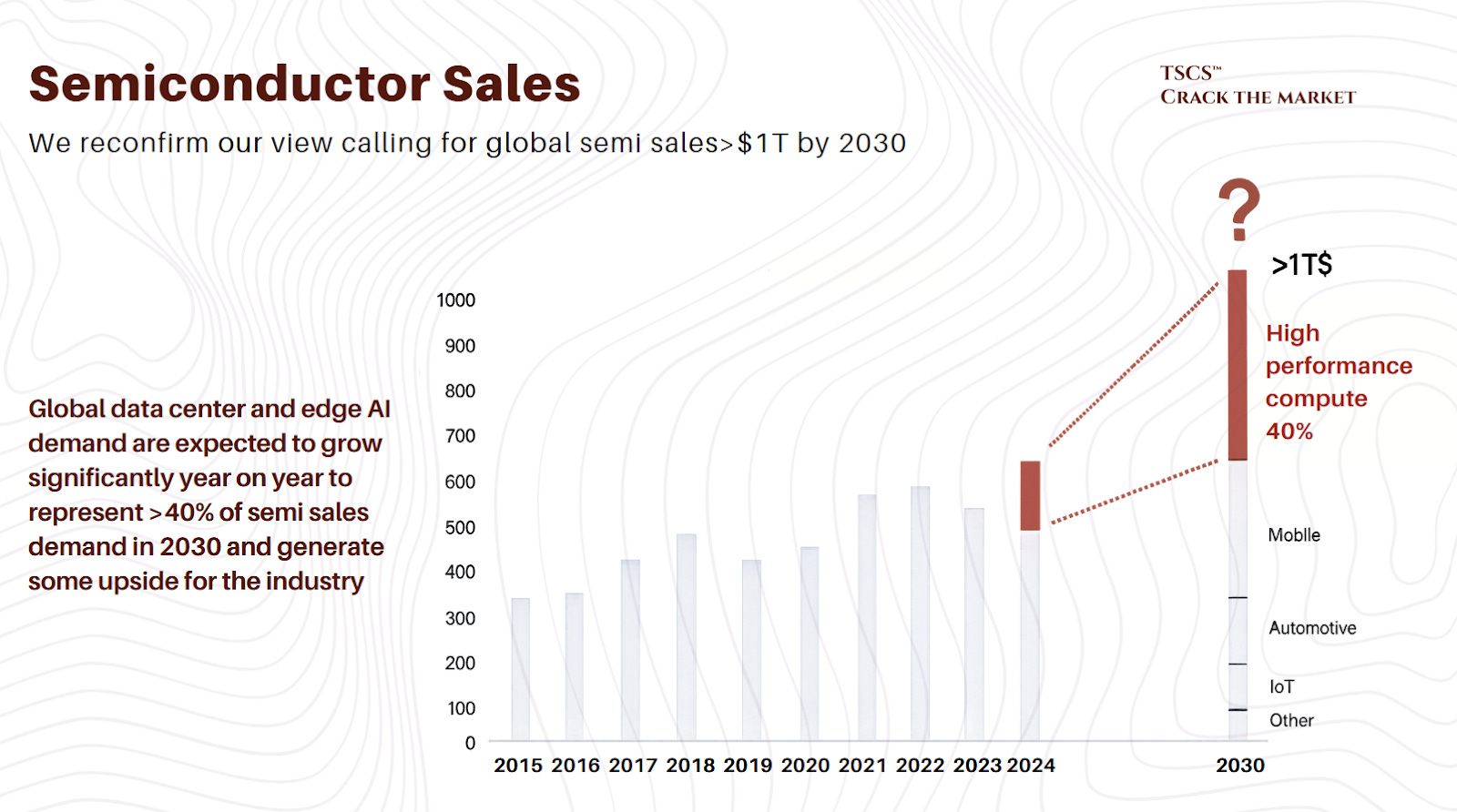
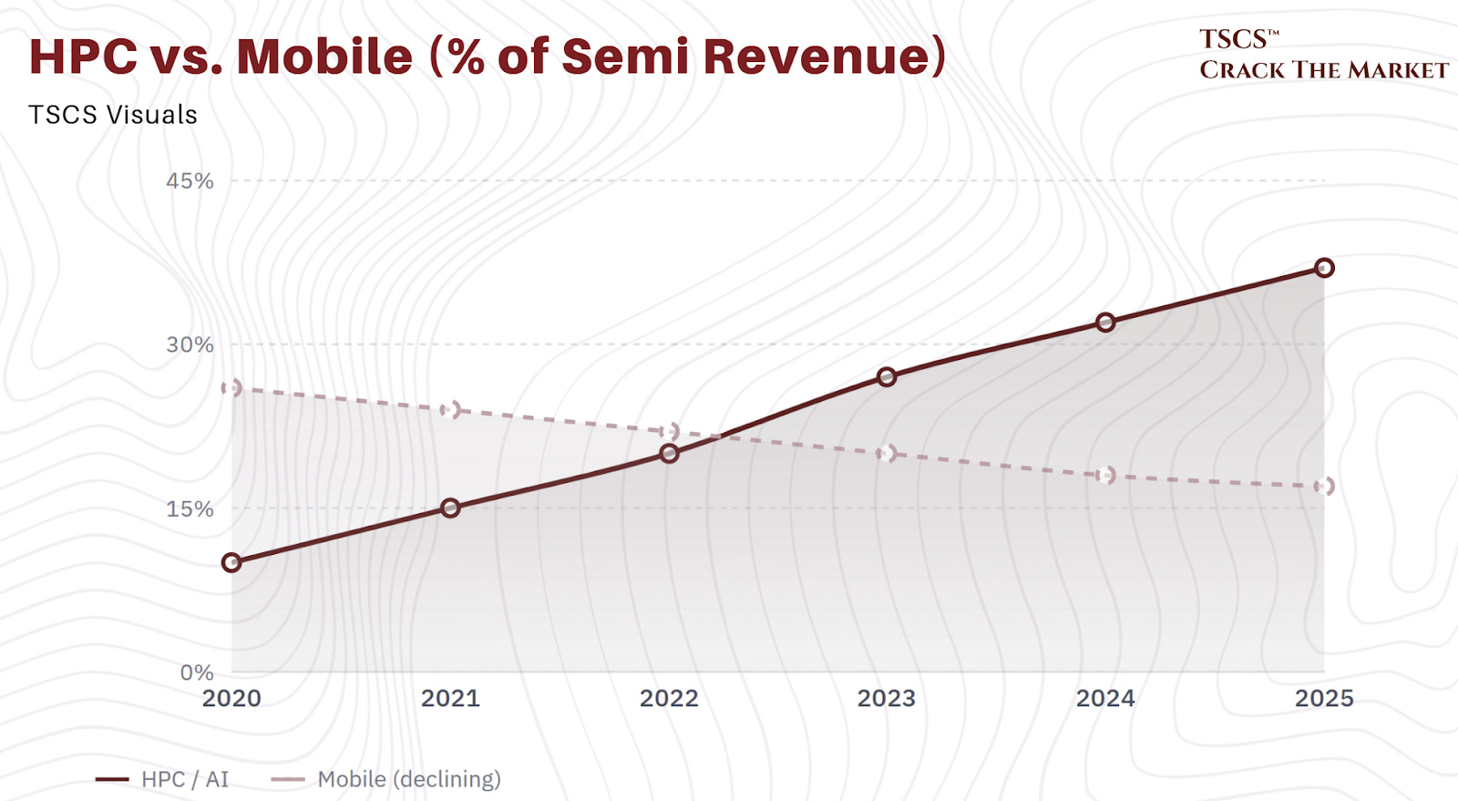
The shift is dramatic. HPC (High Performance Computing) grew from 10% of core semiconductor revenue in 2020 to 37% in 2025, overtaking mobile’s decline from 26% to 17% over the same period. The customer base has fundamentally changed: from price-sensitive consumers optimizing cost to hyperscalers and enterprises optimizing compute performance at nearly any price. This is not a subtle shift. It is a regime change in who writes the checks and what they are willing to pay.
Our view: The magnitude of this demand regime change is best understood through TSMC’s customer mix. In 2020, Apple (consumer) was roughly 25% of TSMC revenue and HPC/AI was under 10%. By 2025, HPC/AI is approaching 50% and will likely exceed it by 2027. The economic implications are profound: consumer demand is inherently deflationary (every iPhone generation must deliver more performance at roughly the same price), while hyperscaler demand is inherently inflationary (every AI model generation requires more compute at almost any price). When your marginal customer shifts from a teenager buying a Galaxy A-series to Meta’s $65 billion capex budget, the pricing power of every link in the chain, from TSMC’s wafer prices to ASML’s tool ASPs to KLA’s inspection intensity, ratchets upward. This is not a cyclical phenomenon. It is a structural repricing of the entire semiconductor supply chain.
How to build a chip: the WFE taxonomy
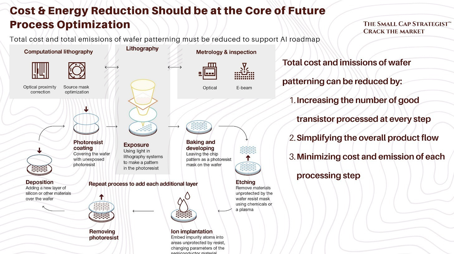
Making a chip is conceptually simple. You draw a pattern (lithography), build structures (deposition), carve away what you do not need (etch), clean up the mess, and repeat. A hundred times. With nanometer precision. On a surface area smaller than your thumbnail.
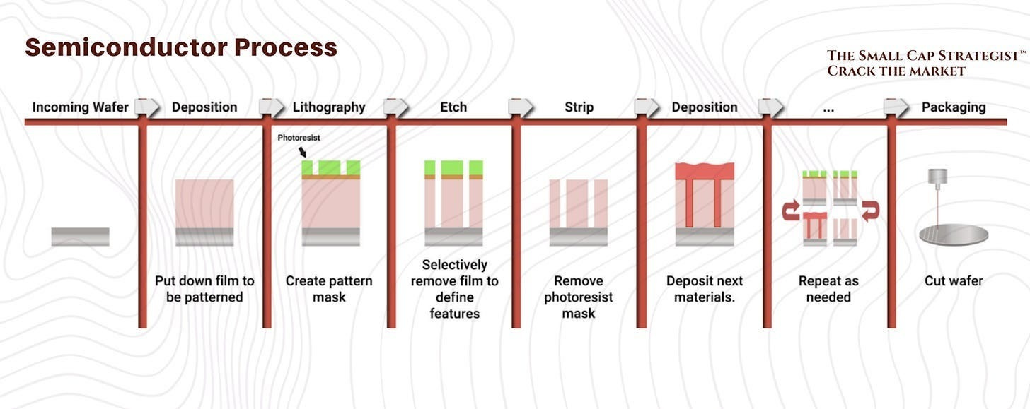
The analogy that works best: chip fabrication is building a city. Lithography draws the blueprints on the ground, showing where buildings, roads, and sewers will go. Deposition and etch actually construct the buildings and roads.
As the city gets denser (smaller transistors), the blueprints require finer resolution (ASML’s EUV). As the buildings get thinner and taller (high-aspect-ratio structures in 3D NAND and GAA transistors), the construction materials and techniques must get more sophisticated (ASMi’s ALD, Lam’s advanced etch).
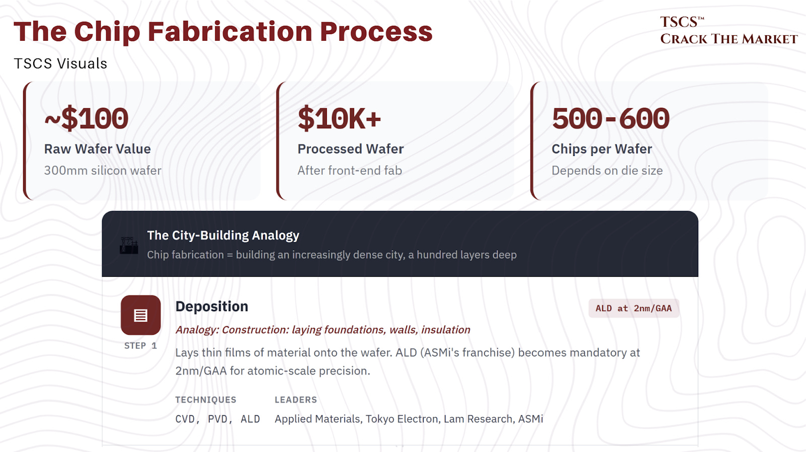
The conversion from a raw silicon wafer (worth roughly $100) to a processed wafer (worth tens of thousands of dollars) containing 500 to 600 chips is the front-end manufacturing process. The subsequent slicing, packaging, and testing of those chips is the back-end. Both require specialized equipment, but the front-end is where the overwhelming majority of WFE spending occurs.
The steps that matter for investors:
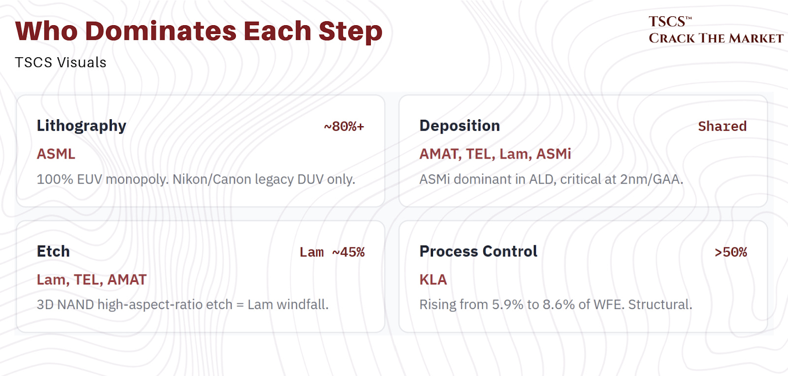
Deposition lays thin films of insulating, conductive, or semiconducting material onto the wafer. Chemical vapor deposition (CVD), physical vapor deposition (PVD), and atomic layer deposition (ALD) are the three techniques. Applied Materials, Tokyo Electron, Lam Research, and ASMi dominate. ALD is the critical one to watch: as transistor geometries shrink to atomic scales, only ALD can coat surfaces with the precision required. This is ASMi’s franchise, and it becomes mandatory at 2nm/GAA.
Lithography transfers circuit patterns onto the wafer using light. This is the step that determines how small your features can be, and therefore how many transistors you can fit per chip. ASML owns this step. Nikon and Canon compete in older DUV tools, but EUV is ASML alone.
Etch removes material to carve the patterns lithography defined. Lam Research, Tokyo Electron, and Applied Materials. The harder the etch (deeper, narrower, higher aspect ratio), the more valuable the tool. This is why 3D NAND, where channels must be etched through 200+ stacked layers, has been such a windfall for Lam.
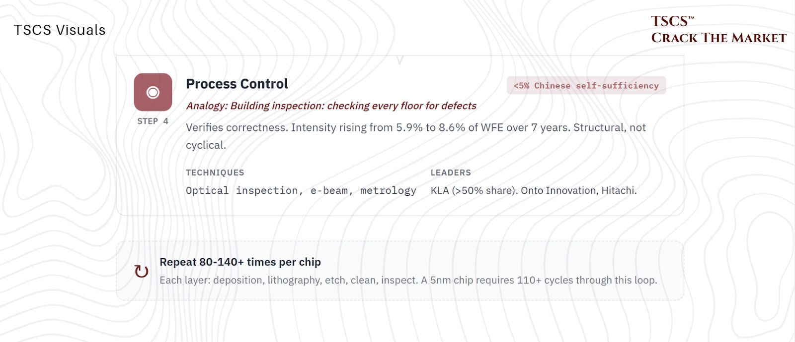
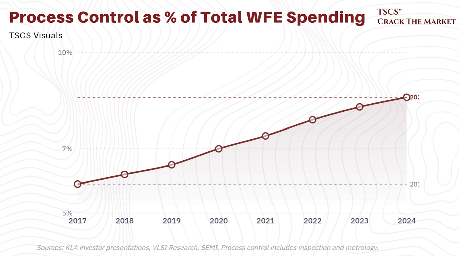
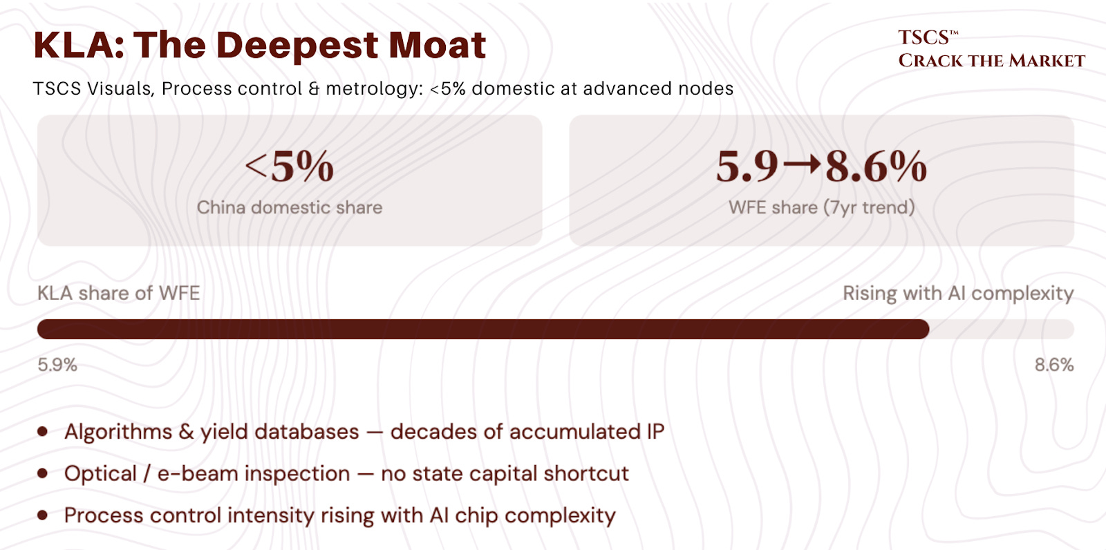
Process control (inspection and metrology) verifies that everything above was done correctly. KLA owns this with over 50% market share. As chips get more complex, the probability of defects per layer rises, and the cost of a defective wafer rises with it. Process control intensity has increased from 5.9% to 8.6% of total WFE over the past seven years. This is not cyclical. It is structural.
TSCS view: Process control intensity rising from 5.9% to 8.6% of total WFE over seven years is one of the most structurally significant data points in the semicap space, and it only moves in one direction. As chips get more complex, more layers and smaller features mean more opportunities for defects and higher costs when defects slip through. KLA’s dominance here is worth understanding in detail, and we return to it extensively in the China section, where the moat’s imperviousness to domestic substitution becomes the central analytical point. For now, note that this is the one equipment category where Chinese self-sufficiency remains below 5% at advanced nodes, and where the barriers to entry are not capital but accumulated decades of proprietary yield data. We will explain why later in this piece.
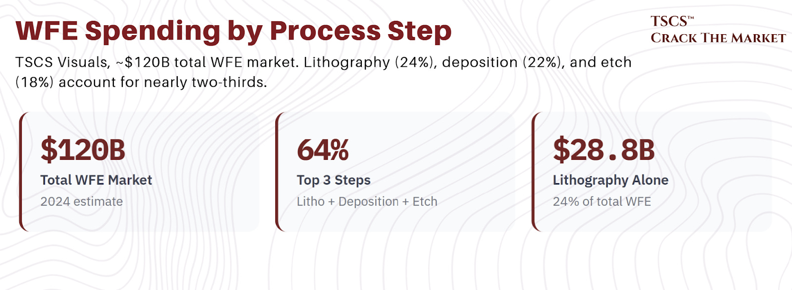
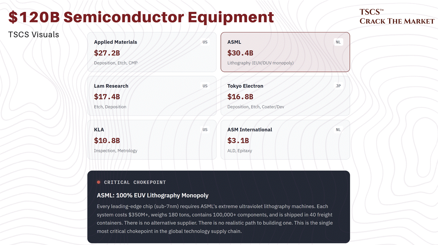
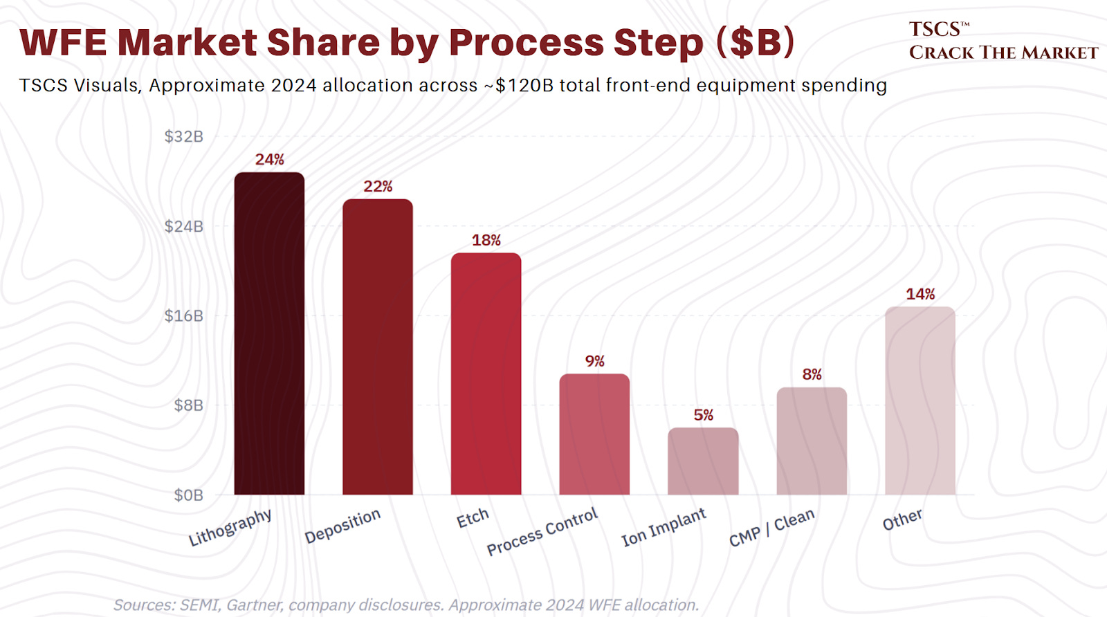
Lithography: the $28 billion bottleneck
Lithography deserves its own treatment because it accounts for 24% of WFE spending and because ASML’s monopoly is the single most important competitive dynamic in the industry.
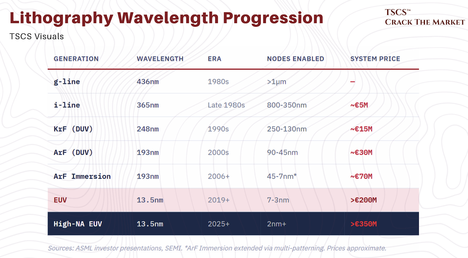
The physics is straightforward: shorter wavelengths of light enable smaller features. The industry progressed from g-line (436nm) through i-line (365nm), KrF (248nm), ArF (193nm), and immersion ArF (193nm through purified water) before arriving at EUV (13.5nm). Each generation enabled a new range of transistor sizes. The problem was that the industry stayed stuck at 193nm wavelength for over a decade while needing to print features at 10nm and below, requiring drawings 20 times smaller than the wavelength of light. Multi-patterning hacks (exposing the wafer multiple times at different angles) kept things going, but at enormous cost and complexity.
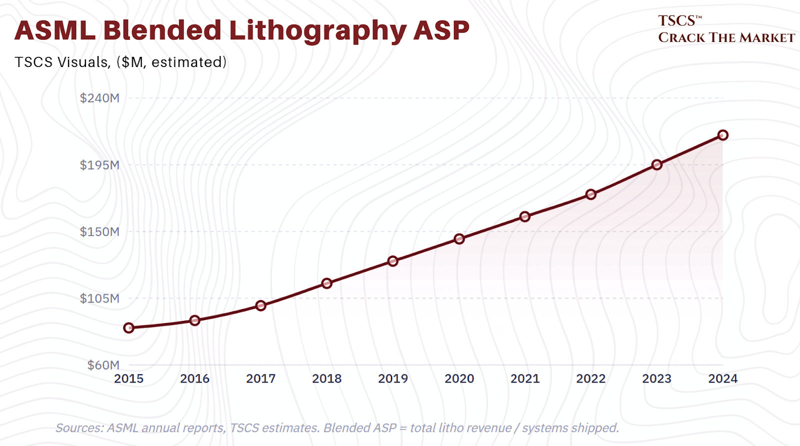
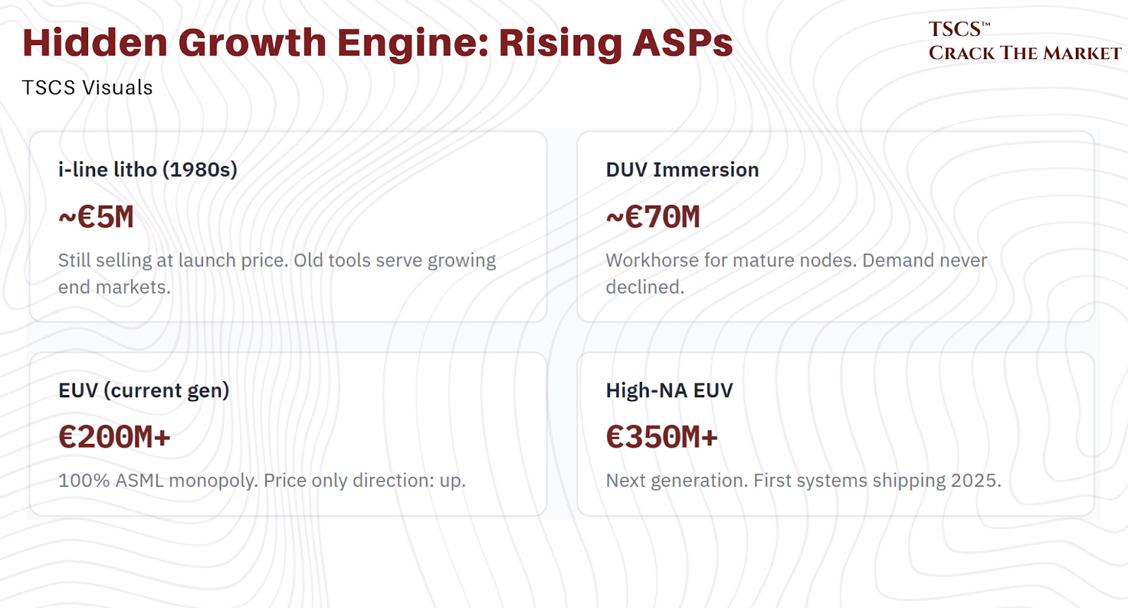
EUV solved this. A 13.5nm wavelength prints features directly at the required scale. ASML is the only company on earth that makes EUV lithography systems. Its current-generation EUV tools cost over $200 million each. Its next-generation High-NA EUV systems exceed $350 million. The blended ASP of ASML’s lithography systems has been rising at 10 to 15% CAGR for years. The price of any lithography generation never falls. I-line systems introduced in the late 1980s at roughly €5 million are still selling at roughly €5 million today.
TSCS view: ASML’s pricing power is not a function of monopoly rent-seeking. It is a function of the value its machines create. A single EUV system costing $200 million enables the production of wafers worth tens of billions of dollars over its lifetime. The tool-to-output ratio is so extreme that customers would pay more, and ASML knows it, which is why ASPs keep climbing. The “nm” designation for chips has become essentially symbolic at this point (a “3nm” chip does not have 3nm features), but what has not become symbolic is the cost curve. Each node transition requires more EUV layers, more passes, more sophisticated optics. As we showed in the capex section, equipment cost per 1,000 wpm has more than doubled in two node generations, and lithography is the single largest contributor to that escalation. For investors, ASML’s question is not “will demand grow?” (it will), but whether the 2026 China revenue decline creates a buying opportunity before the 2027/2028 High-NA ramp fully materializes. We think the answer is probably yes, but the timing is tricky.
Foundries, TSMC, and Foundry 2.0
Thirty years ago, someone had a simple idea: what if semiconductor companies shared factories instead of each building their own? That idea created the foundry model, and the foundry model created TSMC, and TSMC created the modern technology industry. It is not an exaggeration to say that a single company in Hsinchu, Taiwan manufactures the physical substrate on which Western civilization’s digital infrastructure runs.
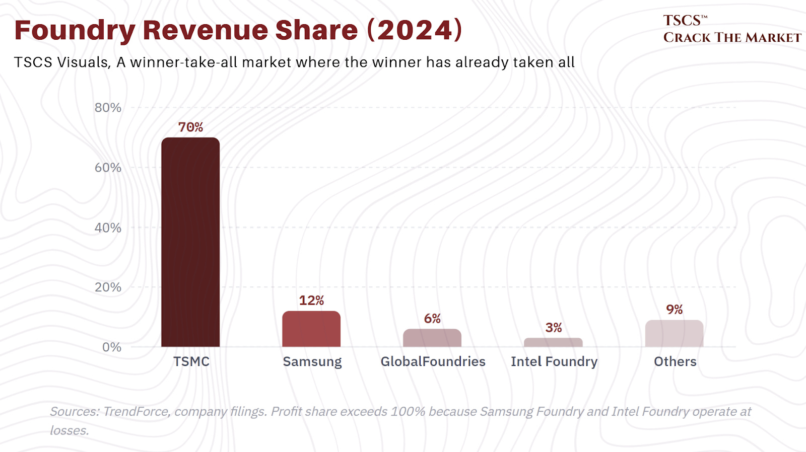
The toll booth of everything
TSMC has 70% revenue share of the global foundry market and over 100% of its profit share (meaning every other foundry, in aggregate, loses money on an economic basis). Samsung’s foundry division has been struggling with disastrous yield rates at 3nm and shut down half its 4nm/5nm/7nm capacity due to chronic operational failures. Intel Foundry is still more aspiration than business. GlobalFoundries exited the leading-edge race years ago.
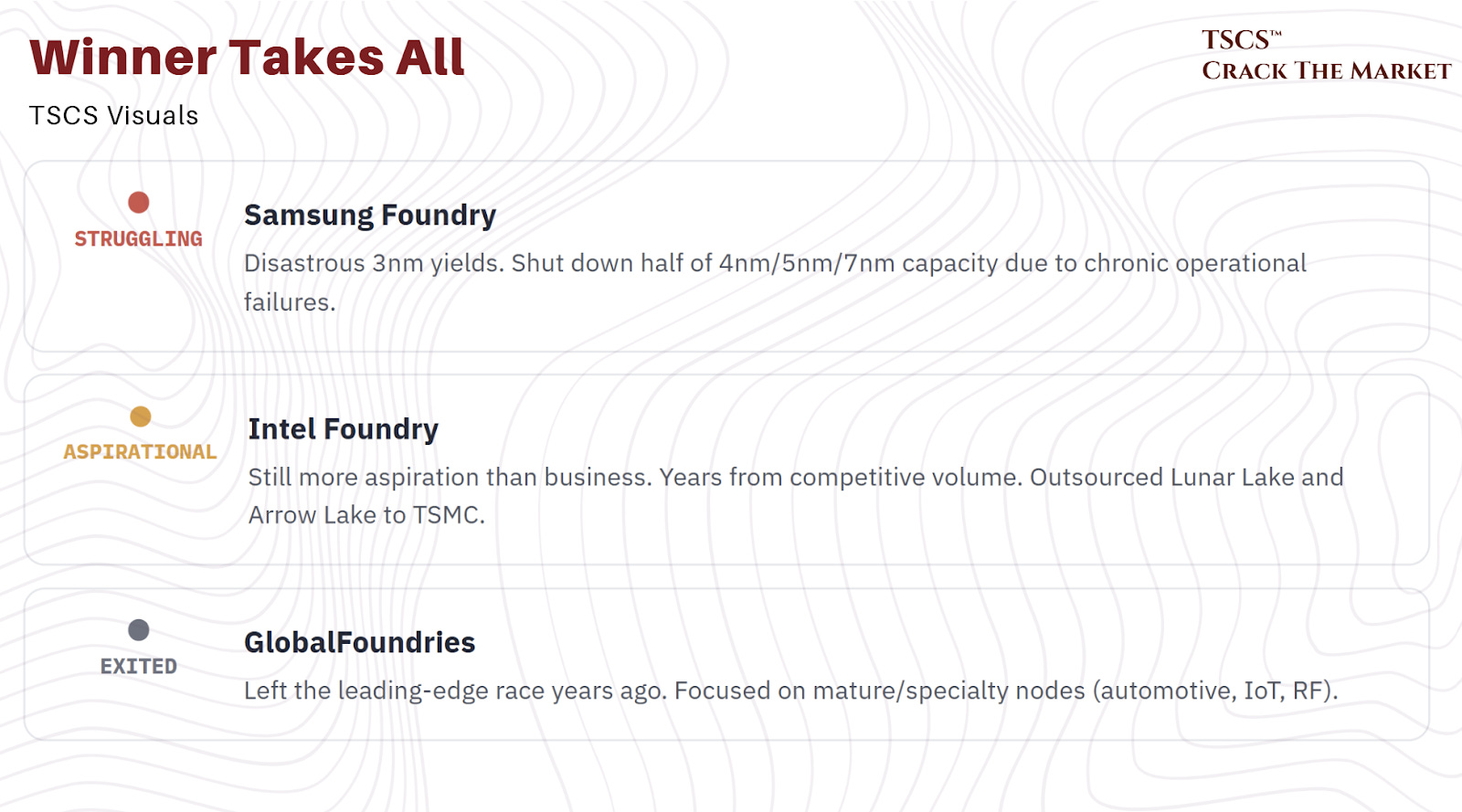
This is a winner-take-all market, and the winner has already taken all.
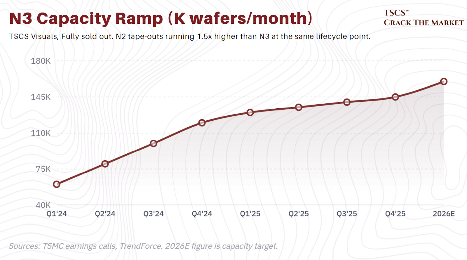
TSMC’s N3 process (3nm) is the most advanced manufacturing technology available to the entire technology industry. Every company that matters has based its next-generation products on it: Apple’s A19, Nvidia’s Rubin, AMD’s MI355X, Google’s Tensor G5. Intel outsourced Lunar Lake and Arrow Lake to TSMC rather than trust its own fabs. N3 capacity has ramped from 60,000 wafers per month to 145,000 by Q4 2025, heading toward 160,000, and it is fully sold out. N2 tape-outs are running 1.5x higher than N3 at the same point in its lifecycle. Apple alone is expected to absorb 70 to 75% of initial N2 capacity in 2026.
Our view: The concentration risk in TSMC is something the market simultaneously acknowledges and ignores. Everyone knows that a Taiwan contingency would be catastrophic. Everyone also knows that there is no alternative. Samsung cannot yield advanced nodes. Intel cannot ship on time. The Arizona fabs are years from meaningful volume. So the market prices TSMC as though the geopolitical risk is a tail event and the technological dominance is permanent. Both assumptions are probably correct on a 3-year horizon. On a 10-year horizon, we are less certain. But for the purposes of the semicap investment case, TSMC’s dominance is the single most important demand signal: when TSMC raises capex, equipment companies print money. And TSMC is raising capex aggressively.
The capex escalation
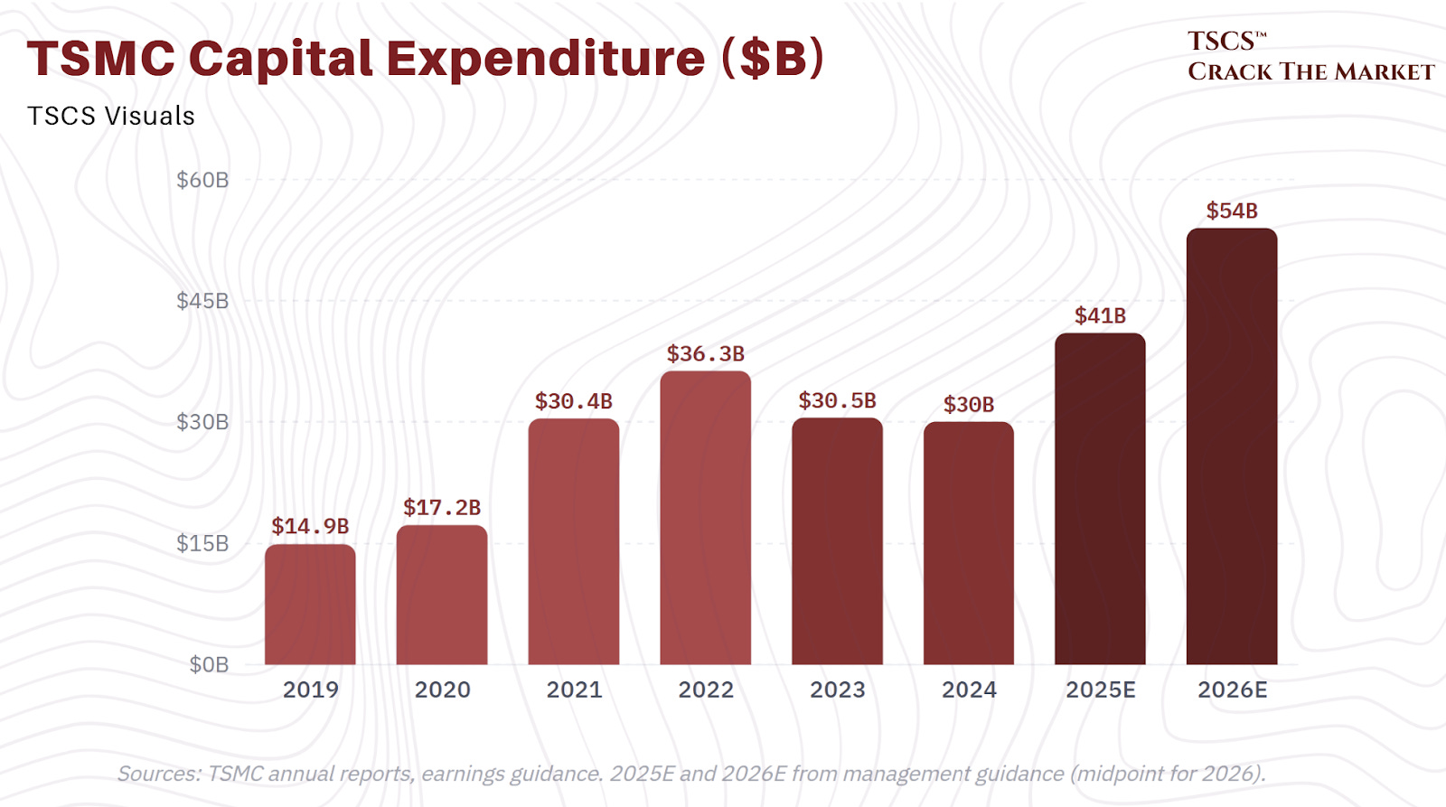
TSMC’s capital expenditure trajectory tells the entire semicap story in one data series. From $30 billion in 2024 to $41 billion in 2025 to $52 to 56 billion in 2026. The last five years totaled $157 billion. The next three years will be, in management’s words, “significantly higher” than the prior three ($101 billion).
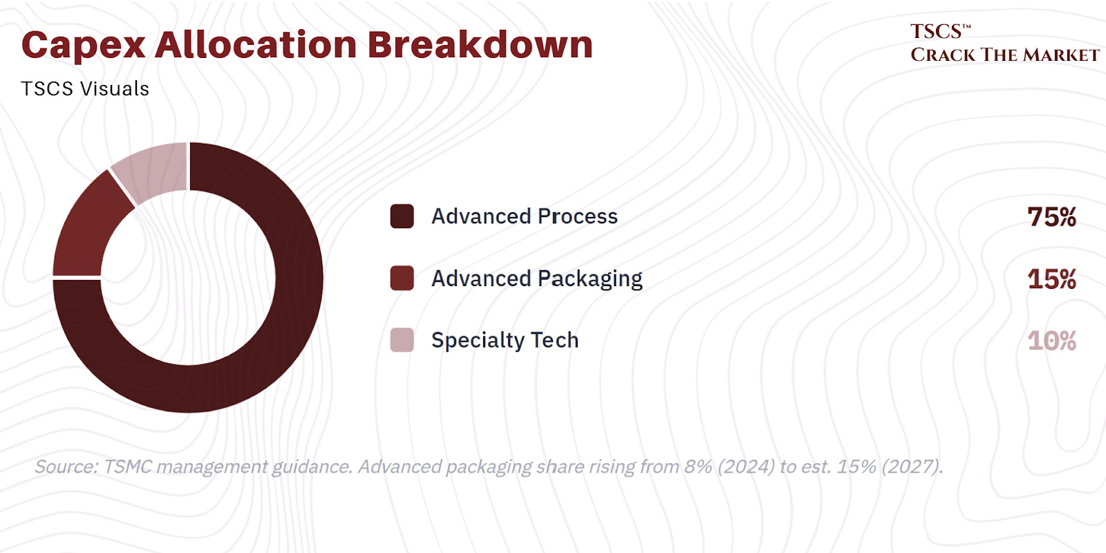
Where is it going? 70 to 80% to advanced process technologies, 10 to 20% to advanced packaging, 10% to specialty technologies.
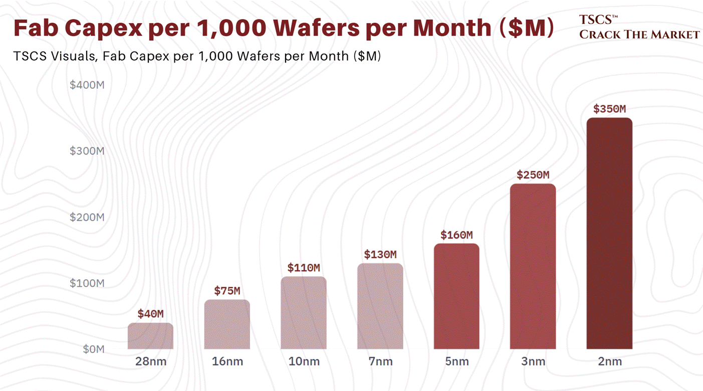
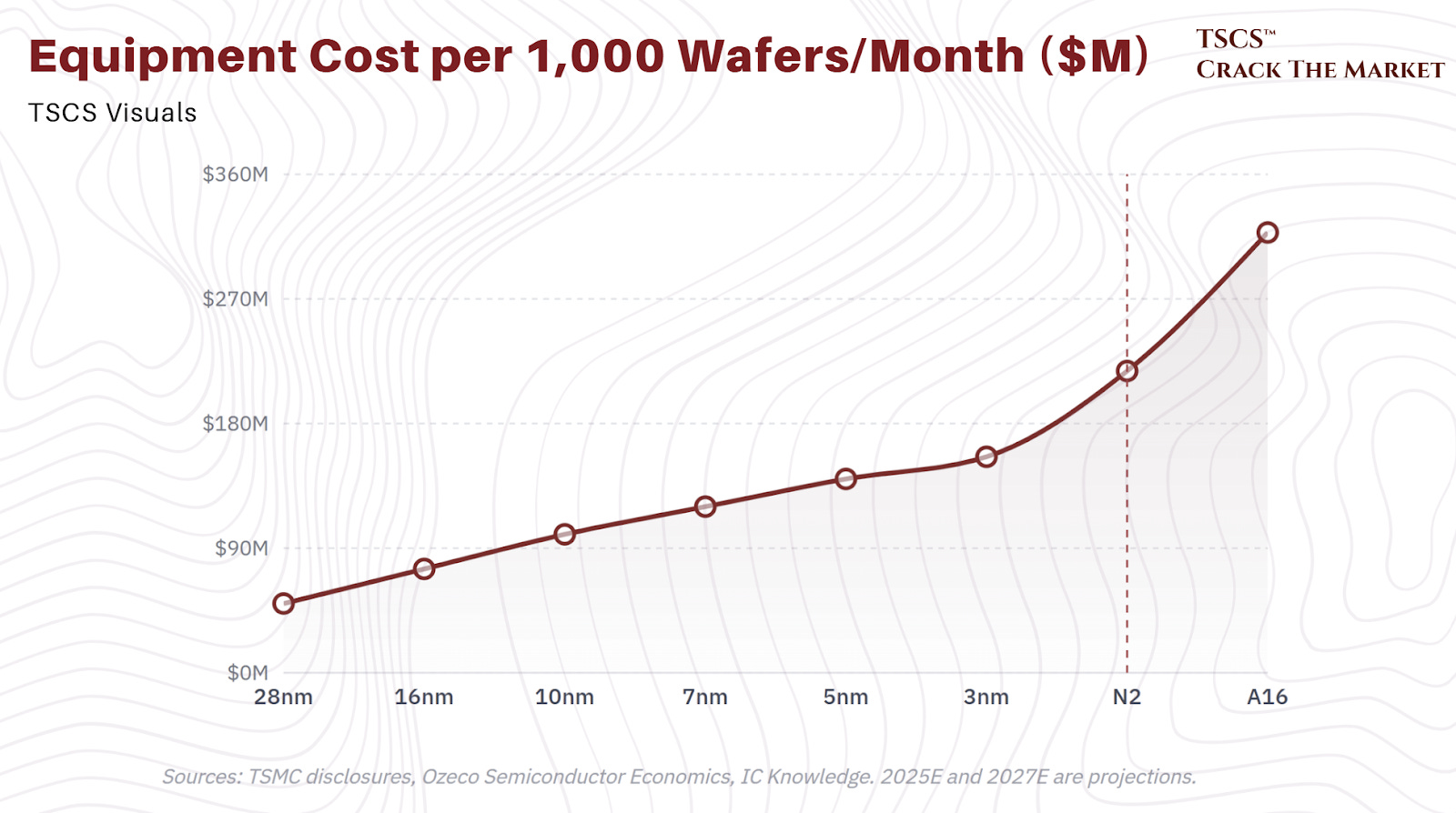
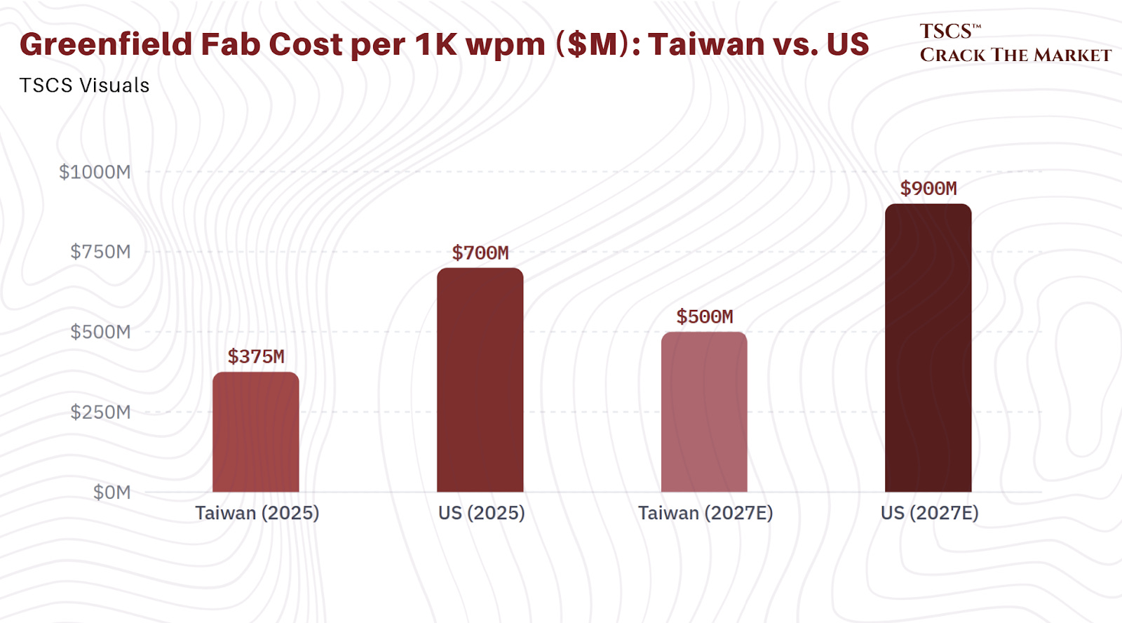
The critical point is that rising capex is not primarily about building more fabs. It is about the rising cost of equipping them. The equipment cost per 1,000 wafers per month of advanced capacity has escalated from $50 million in 2011 to $156 million in 2023 to $218 million in 2025, and is projected to reach $318 million by 2027. At 2nm, a single 1,000 wpm increment costs $350 million in equipment versus $250 million at 3nm and $160 million at 5nm. A greenfield fab with 1,000 wpm of advanced capacity costs $350 to 400 million in Taiwan and up to $700 million in the US today. By 2027, those figures rise to $500 million and $900 million respectively.
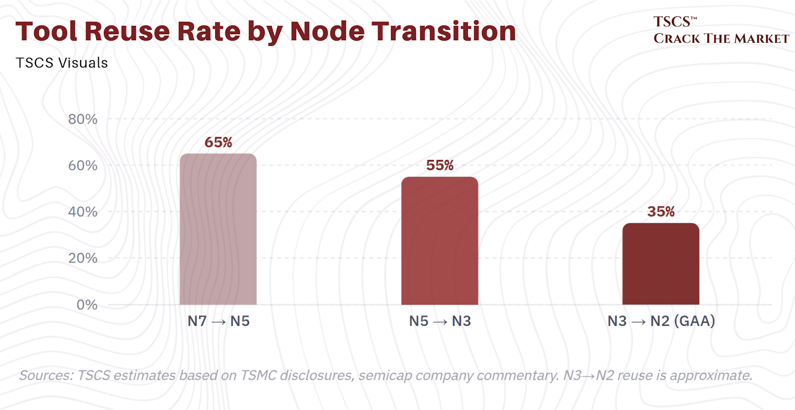
Tool reuse, the practice of repurposing equipment from one node generation to the next, has historically run at 50 to 70% between FinFET nodes (N7 to N5, N5 to N3). At N2, reuse drops substantially because of the Gate-All-Around transistor transition and the introduction of backside power delivery. Lower reuse means more new tool purchases, which means more revenue for equipment companies per unit of capacity added.
Our view: The capex escalation data tells you everything you need to know about the semicap investment case in one chart. Equipment cost per 1,000 wpm rising from $160 million at 5nm to $350 million at 2nm is not inflation. It is physics, specifically the physics of the GAA transistor transition and the introduction of backside power delivery, both of which we detail in the technology section below. The critical implication is that tool reuse, the practice of repurposing equipment across node generations, drops substantially at N2 because the transistor architecture itself is changing. At FinFET nodes (7nm through 3nm), reuse ran at 50 to 70%. At N2/GAA, that figure falls meaningfully, and every percentage point of lost reuse translates directly into incremental equipment purchases. This is a step-function increase in equipment intensity that consensus WFE forecasts, which embed a smooth “9% CAGR,” have not fully captured. The companies most levered to this dynamic are ASMi (ALD becomes mandatory at GAA), AMAT (materials engineering gains share), and KLA (inspection complexity rises with architectural novelty). We unpack each of these in the technology and investor sections.
Foundry 2.0: TSMC is no longer a foundry
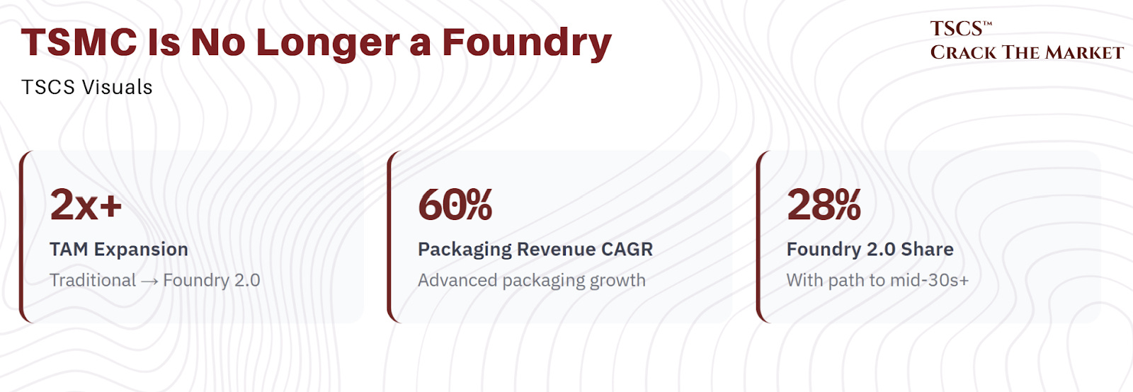
The traditional definition of a foundry is a contract manufacturer that prints chips on wafers. TSMC has outgrown that definition entirely. Under its “Foundry 2.0” framework, TSMC now co-designs chip architectures with customers, manufactures leading-edge logic, integrates memory, performs advanced packaging (CoWoS, InFO, SoIC), stacks dies in 3D, tests complete systems, and guarantees performance. Customers are no longer buying wafers. They are buying finished computing systems.
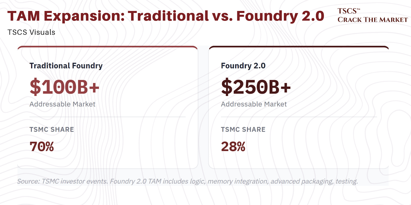
The TAM implications are significant. Under the traditional foundry definition, TSMC has over 70% market share of a relatively narrow market. Under Foundry 2.0, the addressable market more than doubles, and TSMC’s share starts at 28% with a clear path to the mid-30s and beyond. Advanced packaging revenue alone is expanding at a 60% CAGR, growing from 8% of TSMC sales in 2024 to an estimated 15% by 2027.
Our view: Foundry 2.0 is not marketing. It is a structural expansion of TSMC’s economic moat. We detail the specific packaging technologies, CoWoS, SoIC, and hybrid bonding, and their equipment implications in the packaging section below. and making itself even more indispensable to customers. A hyperscaler designing a custom AI ASIC does not want to coordinate between a foundry for logic, a separate company for packaging, and a third for testing. It wants one throat to choke, and TSMC is volunteering for the job. The semicap implication is that back-end equipment spending (bonding, grinding, testing) increasingly flows through TSMC’s capex budget rather than OSAT budgets. Since TSMC spends more aggressively and at higher technological intensity than OSATs ever did, this consolidation is net positive for equipment companies serving the back end, particularly Advantest (testing), Disco (grinding), and Besi (hybrid bonding). The value chain is not just growing. It is concentrating, and concentration favors the equipment suppliers selling into the most aggressive buyer.
Semiconductor equipment: the picks and shovels
Every gold rush has its shovel sellers. The difference with semiconductors is that the shovel sellers have monopolies, 70% gross margins, and customers who cannot switch without shutting down a $20 billion fab for six months.
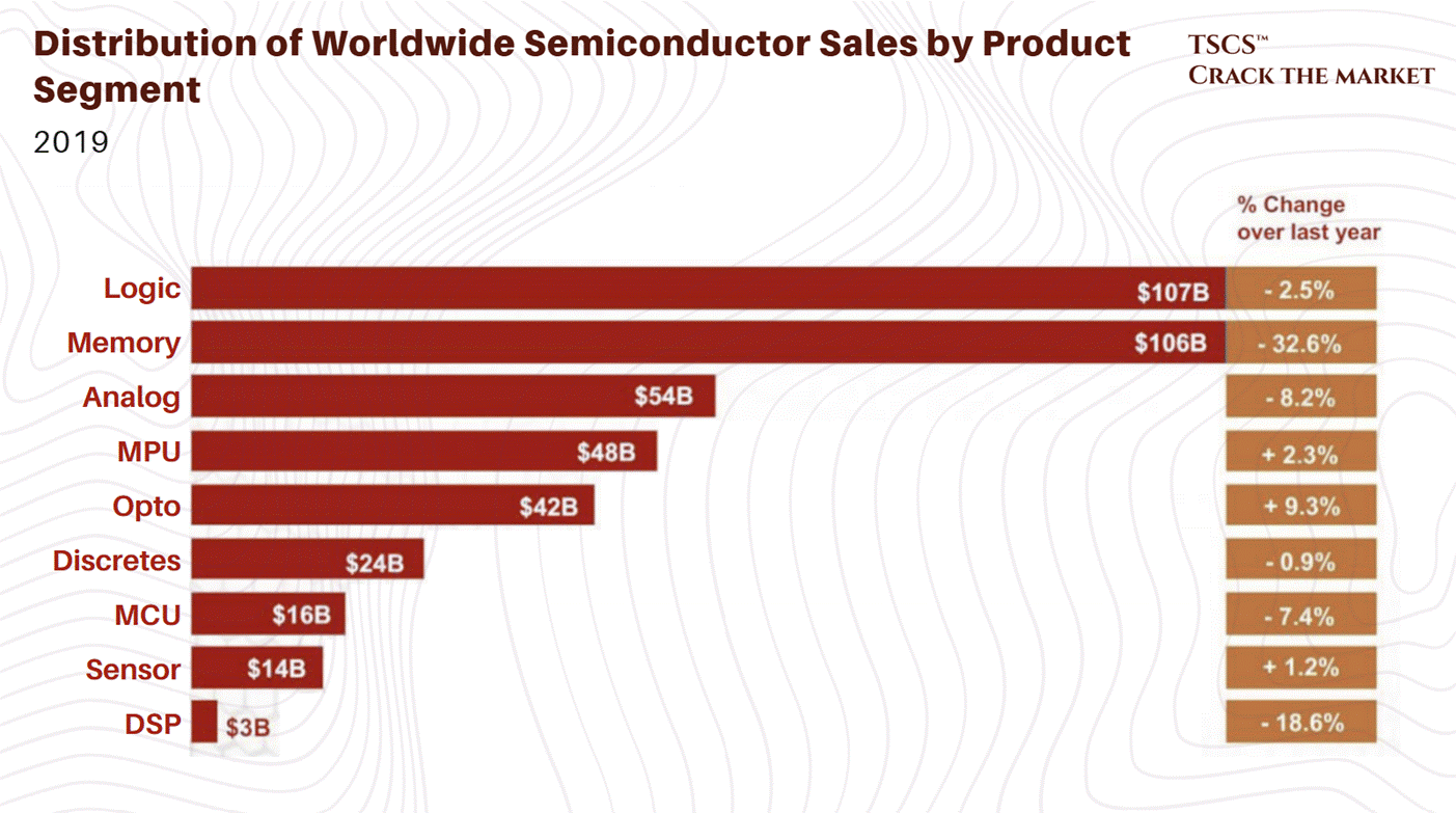
The $120 billion WFE market
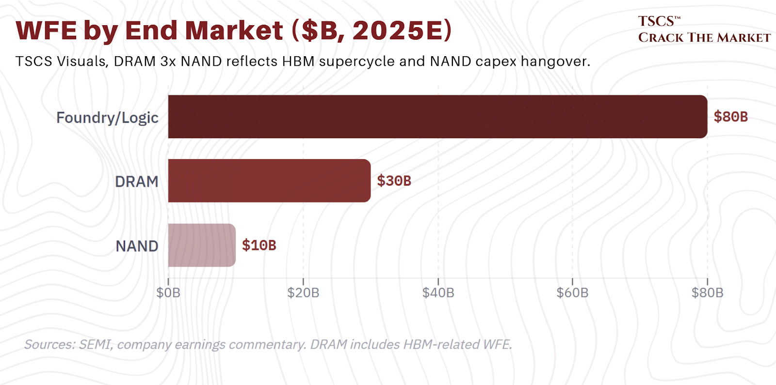
Global wafer fab equipment spending hit roughly $120 billion in 2025, up from $50 billion in 2019, and is projected to reach $155 billion by 2028 at a high-single-digit CAGR. The market splits cleanly into two buckets: memory WFE (over $40 billion, one-third of total) and foundry/logic WFE ($80 billion, two-thirds). Within memory, DRAM dominates at $30 billion versus NAND at $10 billion, a ratio that reflects both the HBM supercycle and NAND’s continued capex hangover from years of overbuilding.
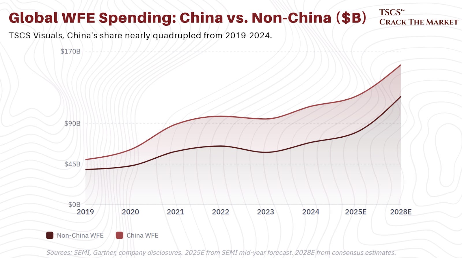
By geography, the split is equally telling: China accounts for $40 billion (up from $11 billion in 2019) and non-China for $80 billion (up from $40 billion). We will deal with the China problem in detail later. For now, note that China’s share of global WFE nearly quadrupled in six years, and that trajectory is about to reverse.
The oligopoly
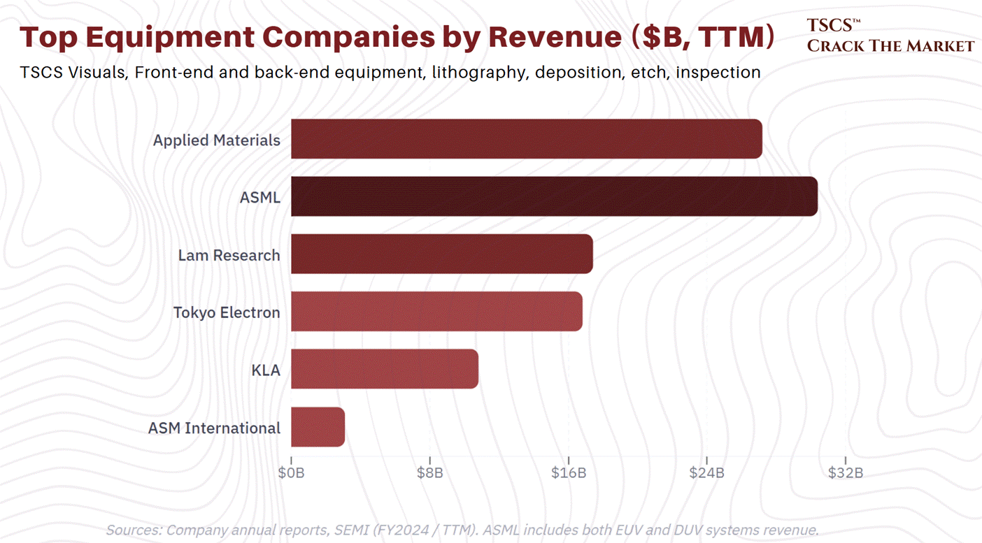
Five companies control roughly 70% of the WFE market, and within their respective niches the concentration is far more extreme:
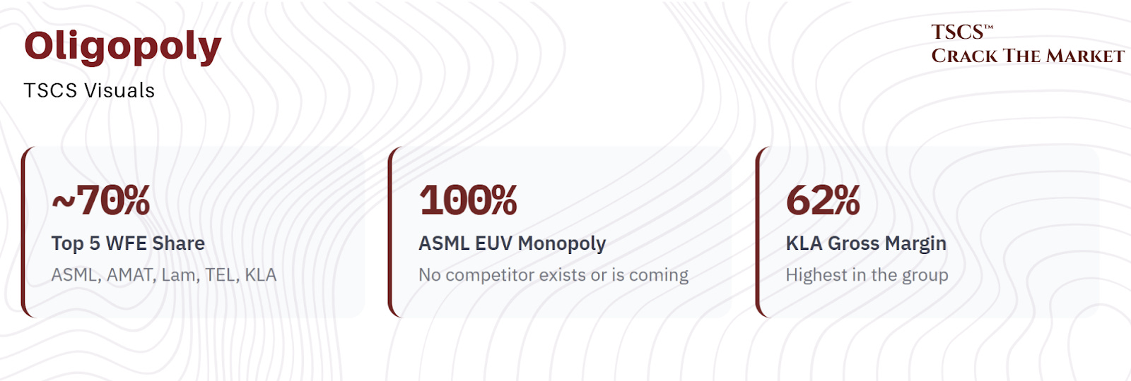
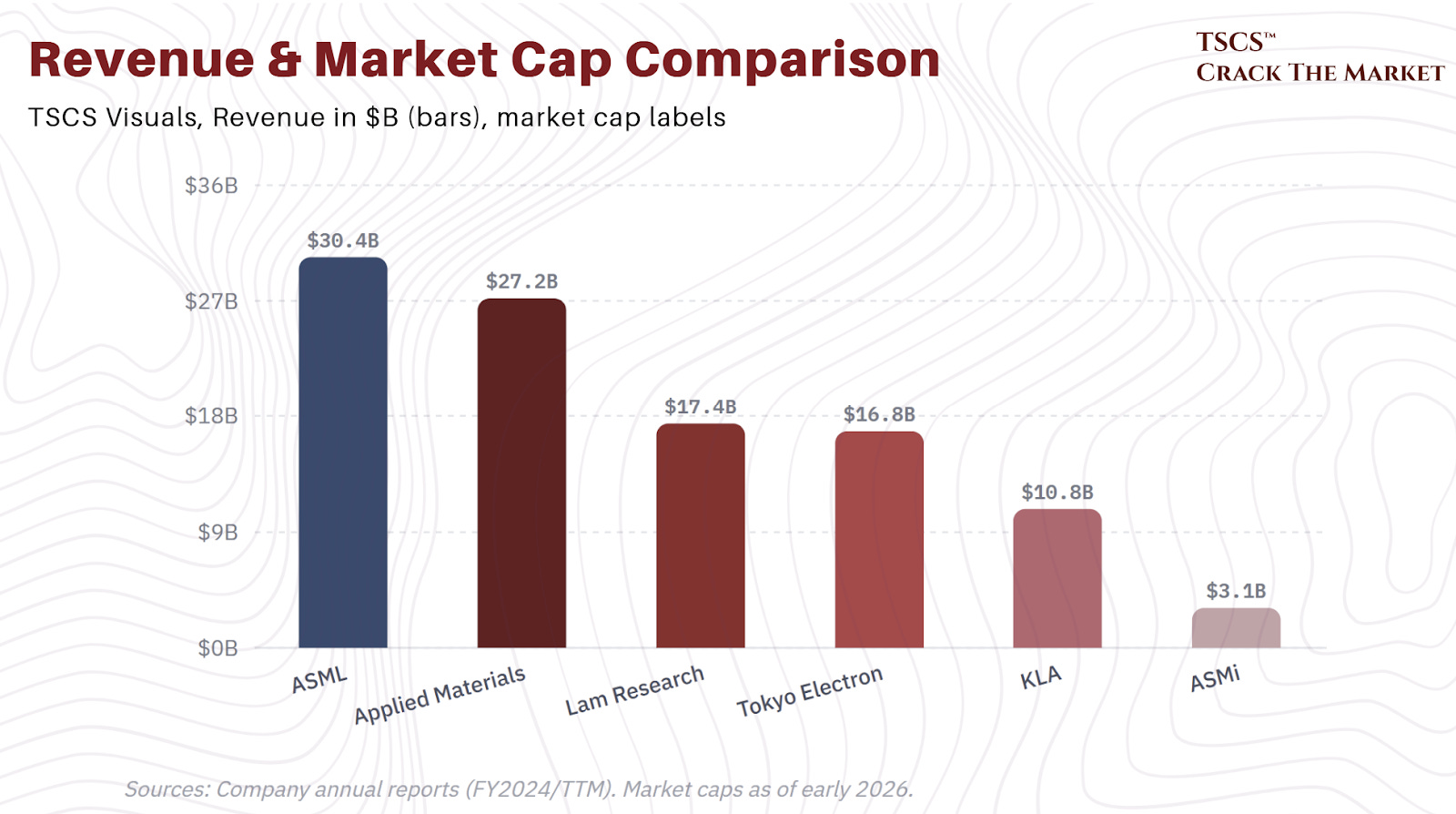
ASML (Netherlands, $525 billion market cap) owns lithography. 100% share in EUV, 90% of total lithography. No competitor exists, none is coming, and the barriers to entry are not financial but physical. ASML’s supply chain alone involves over 5,000 suppliers across 30 countries. You cannot replicate this with capital. You replicate it with decades, and nobody has decades to spare.
Applied Materials (USA, $240 billion) is the generalist. Largest and most diversified supplier across deposition, etch, CMP, and process control. The “materials engineering” positioning gives it unique exposure to the GAA transition and advanced packaging. Lower China concentration than peers at roughly 30% of revenue.
Lam Research (USA, $260 billion) is the memory specialist. Dominant in etch and deposition for 3D NAND, where high-aspect-ratio etching through 200+ layers is its franchise. The highest-beta play on a memory capex recovery, which is both its opportunity and its vulnerability.
Tokyo Electron (Japan, $120 billion) is the diversified Japanese champion. Strong across track (coating/developing), etch, and deposition, with a growing position in hybrid bonding for back-end packaging. Has benefited enormously from Chinese demand filling gaps left by US export controls on American suppliers.
KLA (USA, $175 billion) owns process control. Over 50% share in inspection and metrology, rising toward 60% at advanced nodes. Highest gross margins and operating margins in the group. The only semicap company whose China business is essentially immune to domestic substitution, because the substitution does not exist.
ASMi (Netherlands, $40 billion) rounds out the key players as the ALD monopolist. Smaller than the platform companies but indispensable at the leading edge, where atomic layer deposition is the only technique precise enough to coat GAA transistor structures. A pure-play on Moore’s Law physics.
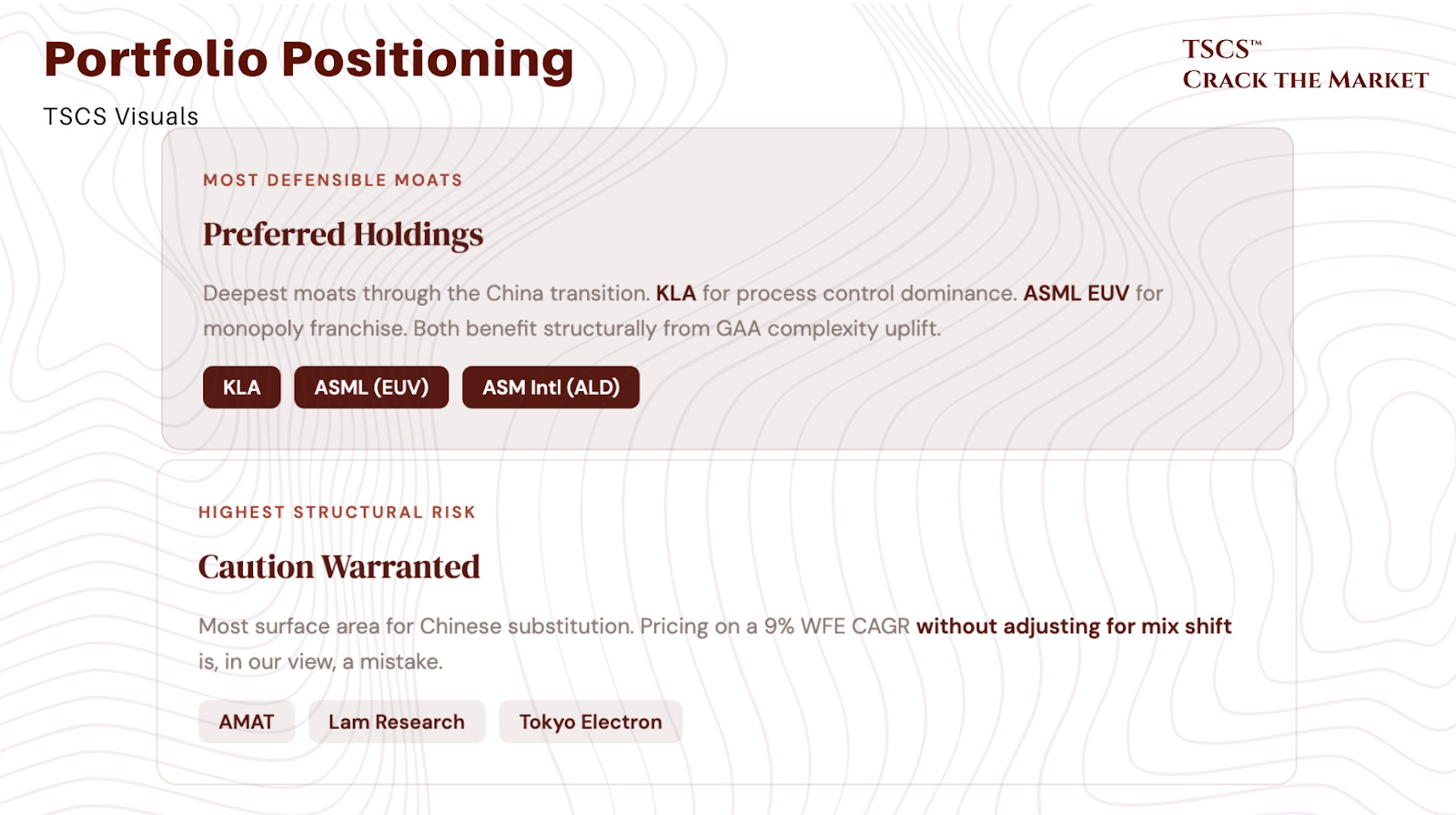
Our view: The semicap oligopoly is, structurally, one of the best competitive positions in global industry. Consider what these companies have in common: (1) customers cannot switch without multi-year requalification cycles, (2) the products are mission-critical with negligible cost relative to the value of the output, (3) consolidation attempts have been blocked (AMAT-TEL, LAM-KLA), meaning the current structure is effectively frozen by antitrust, and (4) Chinese competitors are gaining share in mature-node tools but remain generations behind at the leading edge. This is not a “moat.” It is a geological formation. The question for investors is not whether these are great businesses (they are), but which specific companies are best positioned for the next leg of growth and least exposed to the China risk that Ozeco dissects in detail later in this piece.
The customer concentration problem (that is actually a feature)
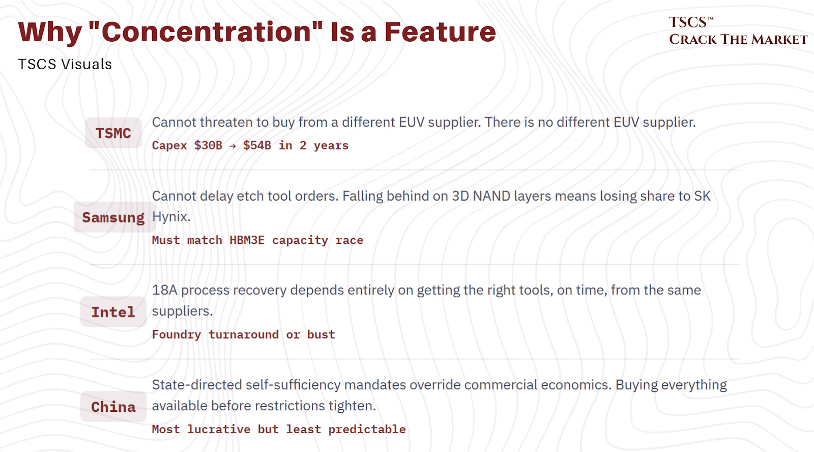
TSMC, Samsung, and Intel represent two-thirds of total WFE demand. Add China’s aggregate spending and you have accounted for nearly the entire market. This looks like dangerous customer concentration until you realize that the customers have no leverage. TSMC cannot credibly threaten to buy from a different EUV supplier because there is no different EUV supplier. Samsung cannot credibly delay its etch tool orders because falling behind on 3D NAND layers means losing share to SK Hynix. The “concentration” runs in both directions, and it runs harder toward the equipment makers.
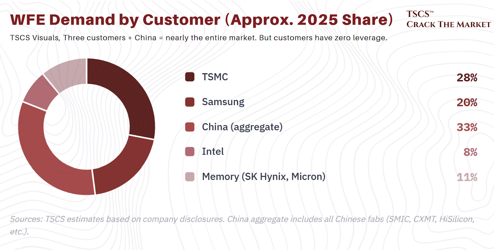
TSMC’s capex trajectory, detailed above, is the single most important leading indicator for semicap revenues. The 2026 figure alone ($52 to 56 billion) exceeds the total WFE market as recently as 2019. When TSMC guides capex up, it is not a forecast. It is a purchase order pipeline. Memory manufacturers (Samsung, SK Hynix, Micron) are the second pillar, with spending rebounding hard on the back of DRAM tightness and the HBM buildout. China is the third, driven by state-directed self-sufficiency mandates rather than commercial economics, which makes it simultaneously the most lucrative and least predictable demand source.
Our view: The semicap “customer concentration” narrative is one of those risks that screens as a red flag in a quantitative model but dissolves under qualitative scrutiny. Yes, TSMC is 25 to 30% of revenue for most equipment companies. But TSMC’s capex budget is a function of AI compute demand, which is a function of hyperscaler capex running at record levels and accelerating. The risk is not that TSMC stops buying. The risk is that TSMC cannot buy fast enough. Equipment lead times for EUV systems are 18 to 24 months. CoWoS packaging capacity is sold out through 2027. The constraint in this market is not demand. It is supply. When your biggest customer is capacity-constrained and desperate for more tools, “customer concentration” is a feature, not a bug.
The hidden revenue stream: services and the installed base
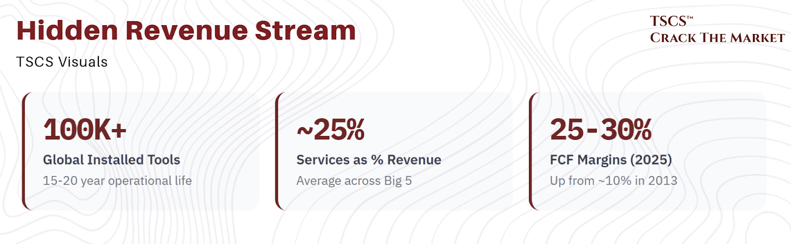
The global installed base of semiconductor equipment exceeds 100,000 tools, each with an operational life of 15 to 20 years. Every tool requires maintenance, spare parts, software updates, and periodic upgrades. This generates a recurring, high-margin revenue stream that most investors underweight in their semicap models, yet it fundamentally changes the character of these businesses.
The numbers are significant and growing. Applied Materials’ AGS (Applied Global Services) segment hit a record $6.4 billion in FY2025, representing roughly 23% of total revenue, with double-digit growth in recurring elements (parts, services, and software). Management noted that AGS operating income alone covers AMAT’s entire dividend payment. ASML’s Installed Base Management revenue reached €8.2 billion in 2025, up 26% year-over-year, accounting for roughly 25% of total sales; management guides IBM revenue growth of over 20% annually as the fleet of advanced EUV tools expands and productivity upgrades (such as the NXE:3800E to full 220 wafers/hour specification) drive service attach. KLA’s services business generated approximately $2.8 billion in its fiscal year 2025 (roughly 22% of revenue), growing at 15% year-over-year, with 75% of services revenue coming from three-year subscription contracts that renew at approximately 95%. KLA generates services revenue equal to 100% of the average selling price of the tool over its lifetime. Lam Research’s CSBG (Customer Support Business Group) runs at roughly $1.7 billion per quarter, with upgrade revenue hitting three consecutive record quarters in 2025 driven by NAND technology conversions.
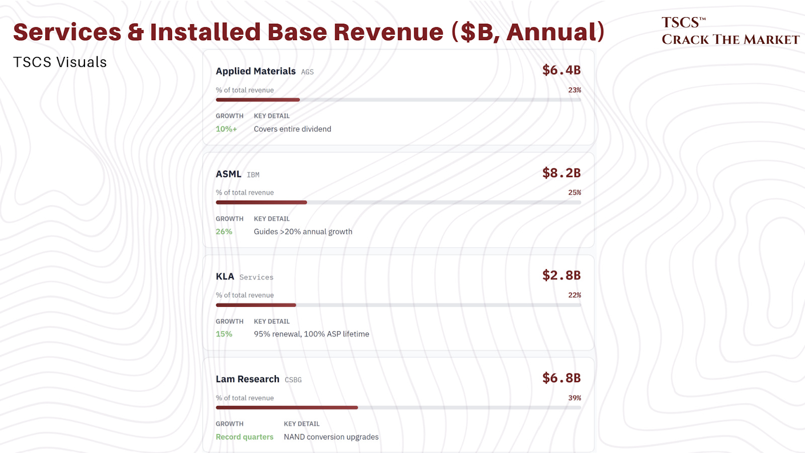
The services flywheel matters for three reasons. First, it provides an earnings floor during cyclical downturns. Services revenue barely declined during the 2019 and 2023 WFE troughs, because fabs that cut new tool purchases still need to maintain and upgrade their existing fleet. Second, it creates formidable switching costs: once a fab is running on your tools, the service relationship locks in for the tool’s operational life. KLA engineers work full-time inside customer fabs like TSMC, providing real-time feedback to KLA’s R&D team, a data loop that no competitor can replicate without decades of embedded presence. Third, the installed base grows every year. Every new tool shipped becomes a future services customer. The compound effect of a growing fleet and rising service attach rates is what converts what looks like a cyclical capital goods business into something closer to a subscription model with a cyclical overlay.
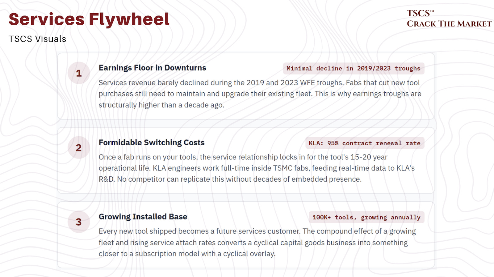
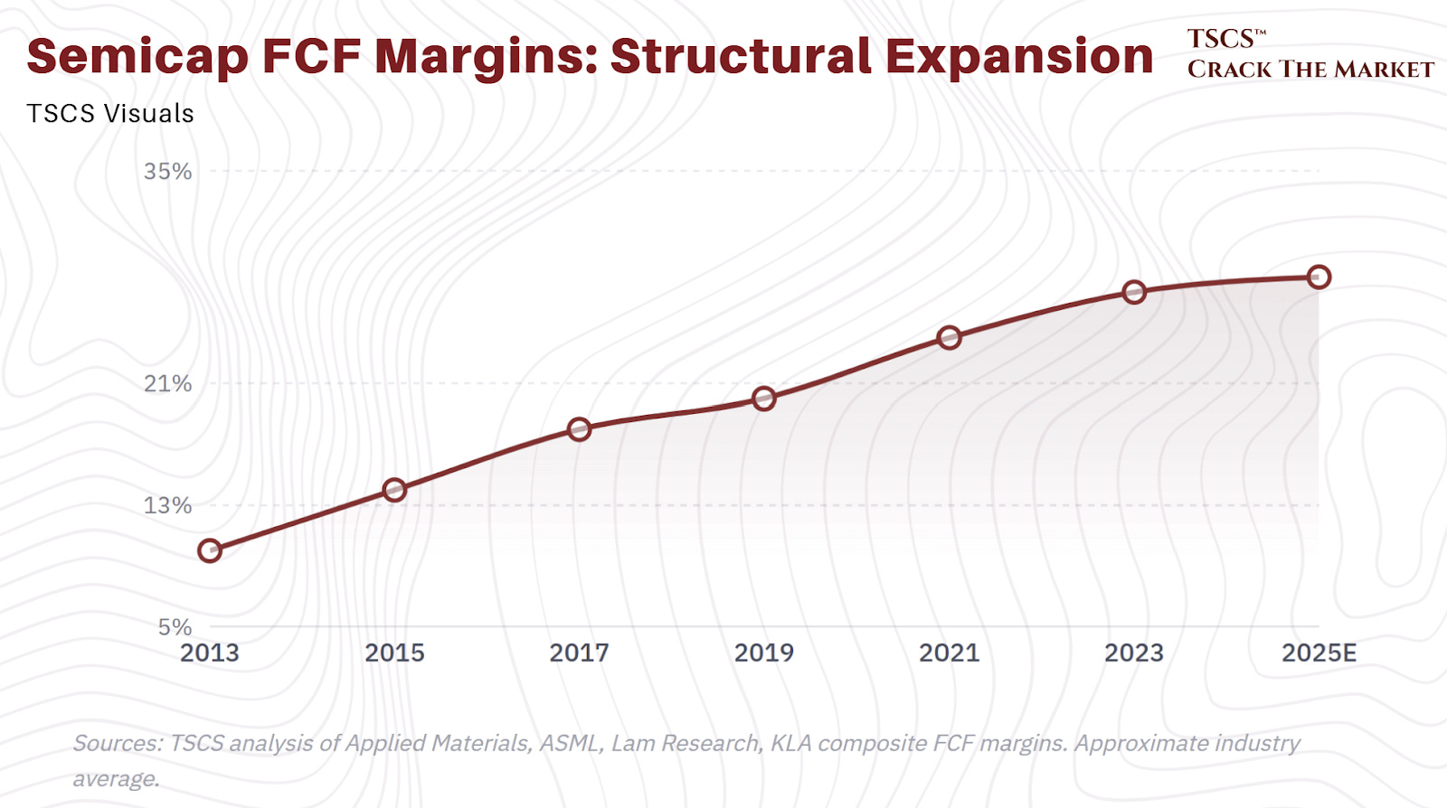
Our view: The services and installed base story is, in our assessment, the most underappreciated component of semicap valuations today. It explains why these companies’ earnings troughs are structurally higher than they were a decade ago, and why FCF margins have expanded from roughly 10% in 2013 to 25-30% today. The China servicing restrictions are eroding this advantage for Western companies in China specifically (ASML must now apply for licenses to service previously sold restricted equipment, and spare parts inventories at Chinese fabs are estimated to last only 3 to 6 months if supply is fully cut). But that makes the non-China installed base even more valuable, because the recurring revenue stream from TSMC, Samsung, Intel, and the memory makers is growing faster than the China service revenue is shrinking. Investors who model semicap companies on system sales alone are missing roughly a quarter of the revenue and the highest-margin quarter at that.
WFE growth drivers for the next decade
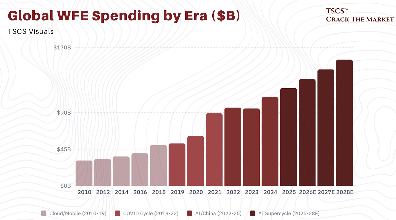
WFE growth is a derivative. Semiconductors grow, foundries build capacity, equipment companies supply the tools. The semiconductor market is growing at 17% CAGR. WFE is growing at 9%. The gap between those two numbers is not a problem. It is a sign of improving capital efficiency, and it means the current spending cycle is more sustainable than the post-COVID binge that preceded it.
Three eras of WFE growth, and the fourth beginning now
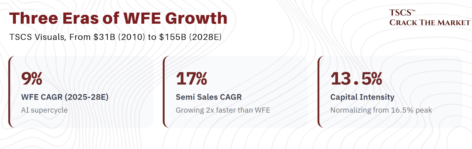
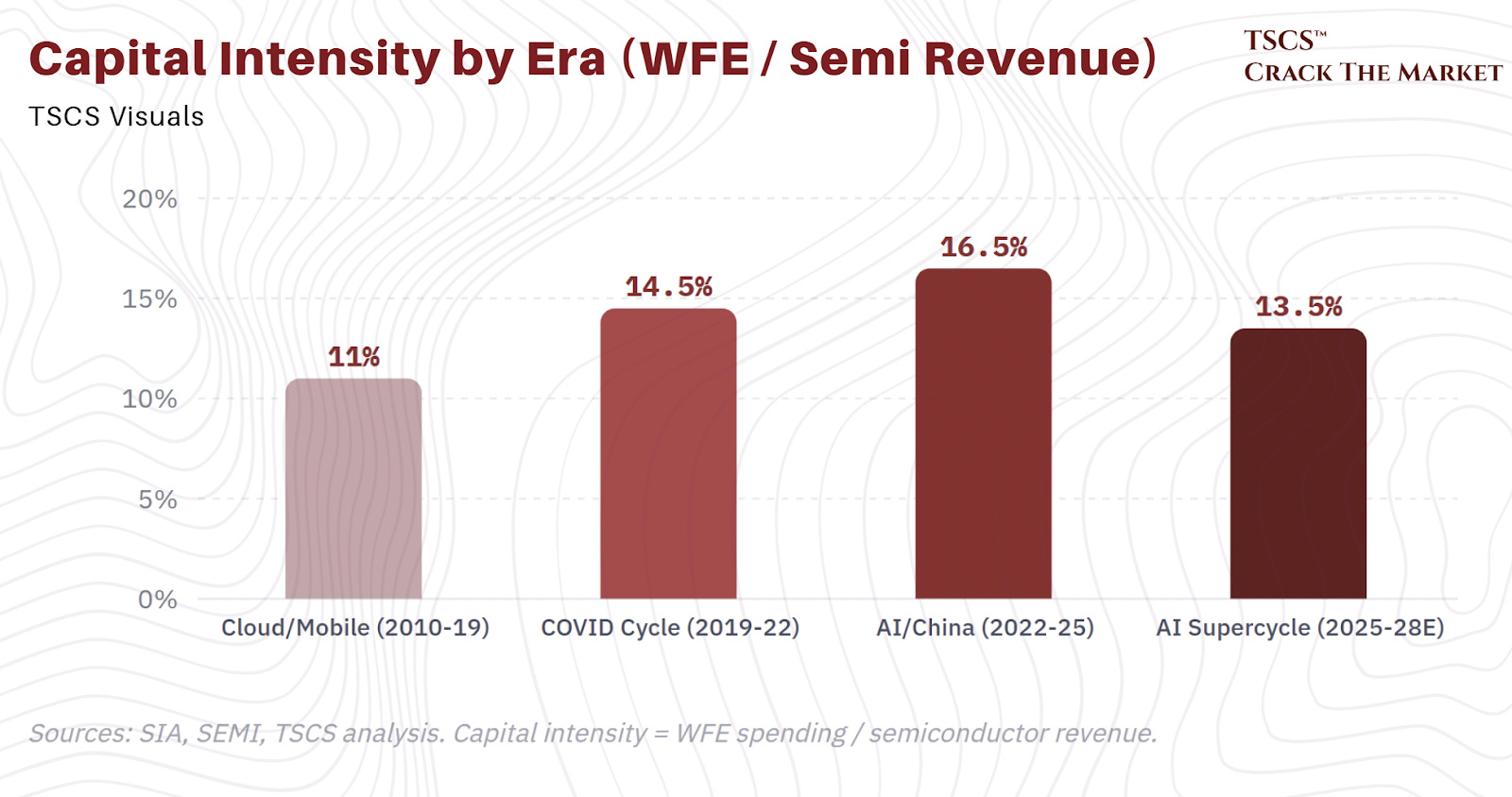
The Cloud/Mobile era (2010 to 2019) took WFE from $31 billion to $52 billion. Steady, unspectacular, driven by smartphone proliferation and the first wave of cloud buildout. Capital intensity averaged 11%.
The COVID cycle (2019 to 2022) took WFE from $52 billion to $96 billion. Nearly doubled the market in three years. Pandemic demand for PCs, servers, and everything digital collided with supply chain panic-buying. Capital intensity spiked to 14.5%. This was not sustainable, and it was not sustained.
The AI/China buildout (2022 to 2025) took WFE from $96 billion to $120 billion. Slower growth (8% CAGR), but the composition shifted dramatically. The best-performing segments were DRAM (HBM plus Chinese expansion), China (pre-buying ahead of export controls), and EUV. This was the transition period where semicaps went from “not AI beneficiaries” to “obviously AI beneficiaries,” a repricing the market only fully recognized in late 2025.
The AI supercycle (2025 to 2028) should deliver at least 9% WFE CAGR, driven by synchronized growth across leading-edge logic (2nm/GAA), HBM, advanced packaging, and reshoring. Capital intensity normalizes to 13.5%. Semi sales growing at 17% on 9% WFE growth means the industry is producing more revenue per dollar of equipment, which is exactly what you want to see if you are worried about overcapacity risk.
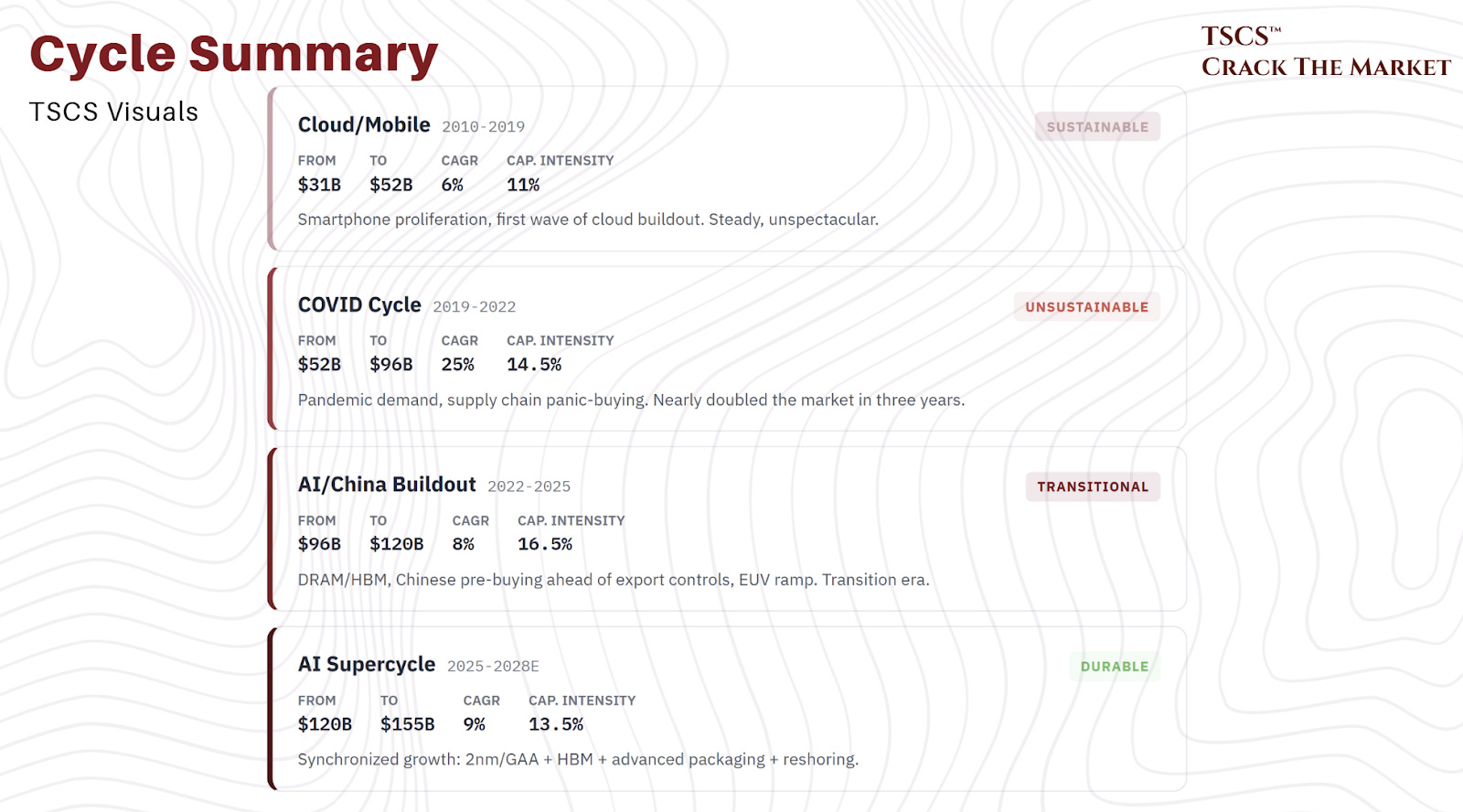
Our view: The capital intensity decline from 16.5% (2022 to 2025) to 13.5% (2025 to 2028) while WFE still grows at 9% is the data point that should settle the “is AI capex sustainable?” debate for anyone willing to do the arithmetic. During the COVID cycle, WFE outgrew semi sales (25% vs. 14.5%), which is the textbook setup for an oversupply hangover. The current cycle is the opposite: semi sales are growing nearly twice as fast as WFE. That means utilization rates stay high, pricing power persists, and the equipment upcycle has duration rather than just amplitude. The 9% CAGR consensus may actually prove conservative if the China risk (which we expect to be a headwind) is offset by faster-than-expected 2nm ramp or an extension of the memory supercycle.
AI: the gravity well
The semiconductor industry’s center of gravity has shifted permanently. Mobile and AI data centers now contribute 70% of industry revenue. HPC grew from 10% of the core semiconductor market in 2020 to 37% in 2025, overtaking mobile (down from 26% to 17%). The customer base flipped from price-sensitive consumers to hyperscalers with functionally unlimited budgets.
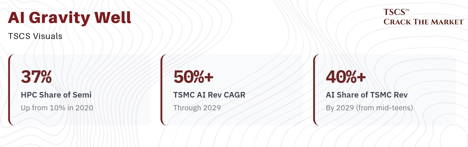
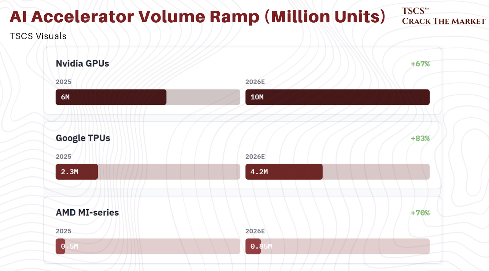
The customer base flipped from price-sensitive consumers to hyperscalers with functionally unlimited budgets. TSMC’s AI accelerator revenue is growing at a mid-to-high 50% CAGR through 2029, grounded in specific customer roadmaps, not vibes. Second, merchant GPU volumes are scaling from 6 million units in 2025 to 10 million in 2026, dominated by Nvidia’s Blackwell with Rubin ramping from H2 2026. AMD’s MI400/450 should add 800,000 to 900,000 units. Google’s Ironwood TPU demand is surging 80% year-over-year to 4.2 million units in 2026, with use cases expanding beyond internal workloads to external customers through TPU leasing and direct hardware sales.
The result: AI data centers are expected to account for 40% or more of TSMC’s total revenue by 2029, up from the mid-teens in 2024.
Our view: We want to be precise about what “AI demand” means for semicap companies, because precision matters when stocks are trading at 30x forward earnings. AI demand for semiconductors is real, verified, and accelerating. But AI demand for WFE is a second derivative, and second derivatives can behave counterintuitively. TSMC growing AI revenue at 50%+ does not mean TSMC’s capex grows at 50%+. It means TSMC’s capex grows at 25 to 30%, of which a rising share goes to advanced nodes and packaging that require more expensive tools. The semicap bull case rests on equipment intensity per dollar of capex rising, not on capex itself growing at the same rate as AI revenue. That distinction matters because it means WFE growth is structurally lower but structurally more durable than the headline AI numbers suggest. We are buying a 9 to 12% grower with monopoly economics, not a 50% grower with commodity economics. Price accordingly.
We should be transparent about an assumption embedded in this analysis. Our AI investment supercycle piece argued that elements of the current AI spending environment resemble bubble dynamics, with capital allocation running ahead of monetization proof points. That view and the semicap bull case are not contradictory, but they are in tension. The reconciliation is timeframe. Even in our most cautious AI scenario, hyperscaler capex sustains above $400 billion annually through 2027, driven by infrastructure contracts already signed, power purchase agreements locked in, and GPU orders placed with 12-18 month lead times. That level of spending is sufficient to drive the WFE cycle we describe. The risk materializes if AI capex retraces to $250-300 billion (a 2022-level reversion), which would break the 9% WFE CAGR assumption and likely compress semicap multiples by 25-30% before earnings estimates adjust. We do not currently expect this scenario, but intellectual honesty requires acknowledging that the semicap bull case is built on the AI capex supercycle continuing, and we have separately argued that supercycle has speculative elements. Investors should size semicap positions with this tension in mind.
Reshoring: the structural tailwind nobody can cancel
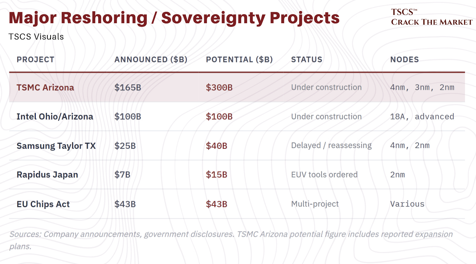
Geopolitics has created a WFE demand source that is independent of commercial supply-demand dynamics. The US is moving toward producing 20 to 25% of all advanced chips domestically, up from near zero. TSMC is spending $165 billion (potentially rising to $300 billion) on its Arizona campus. ASML has received orders from Rapidus, Japan’s new leading-edge foundry. Sovereign investments could add 5 to 8% of extra global capacity for technology sovereignty reasons alone.
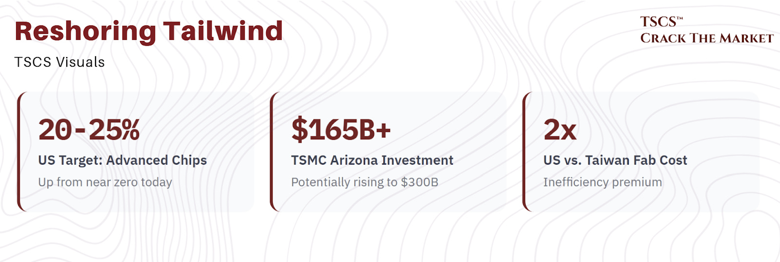
The effect for equipment companies: reshored capacity is structurally less efficient. Subscale fabs without mature local ecosystems require more WFE per unit of output. Building the same wafer capacity in the US costs roughly double what it costs in Taiwan ($700 million versus $350 to 400 million per 1,000 wpm in 2026). The inefficiency premium flows directly to equipment revenue.
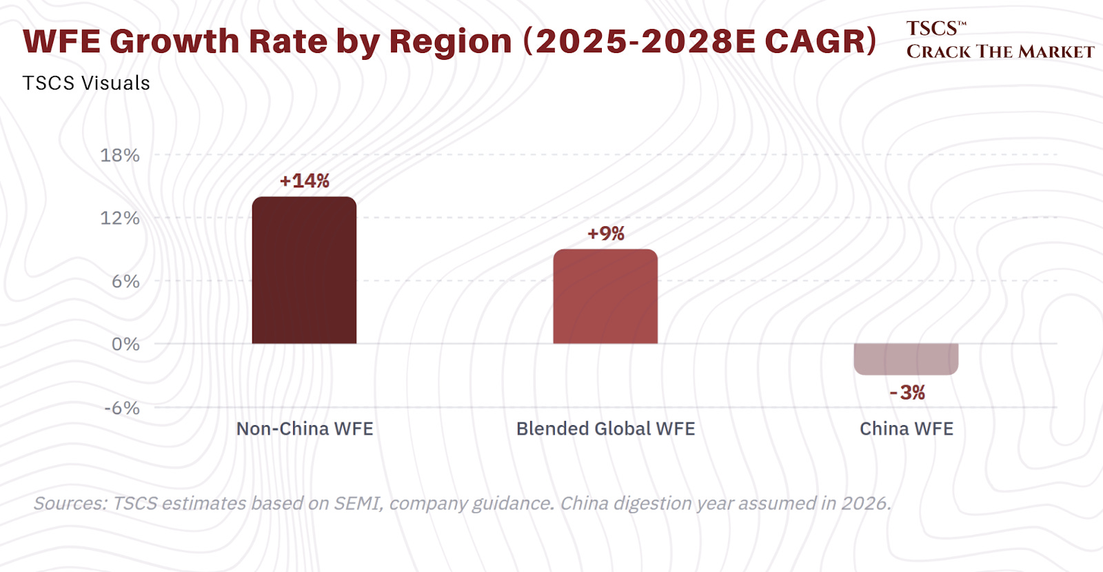
Non-China WFE spending is projected to grow at 14% CAGR from 2025 to 2028, materially faster than the blended 9% rate, as US, European, and Japanese fabs ramp. China WFE may see a digestion year in 2026, though the sustainability of Chinese demand remains the biggest swing factor in any WFE forecast (more on this in the China section).
Node transitions: the gift that keeps giving
TSMC is completely sold out at 3nm and 2nm. Apple, Qualcomm, MediaTek, AMD, Intel, and Nvidia are all competing for capacity on the most advanced nodes because their business models are built on performance leadership. Opting out of the node race would crater their market caps. This competitive dynamic is self-reinforcing: as long as one player transitions, everyone must follow.
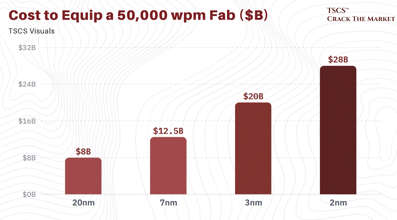
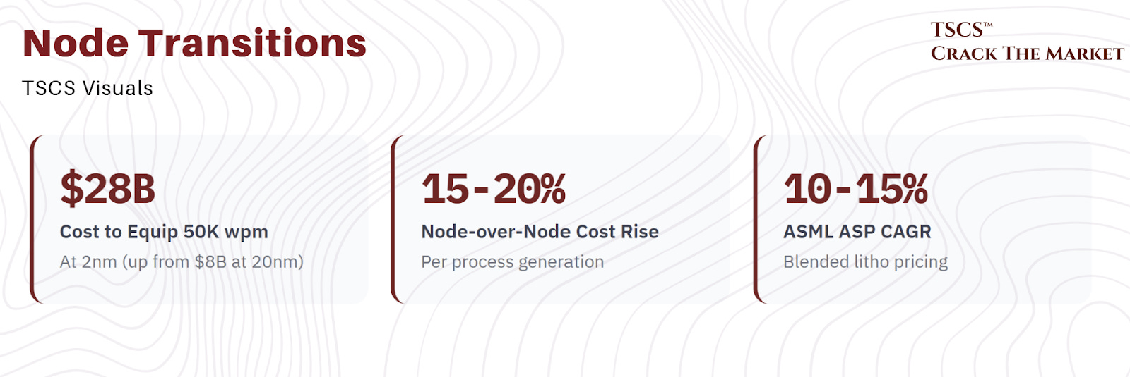
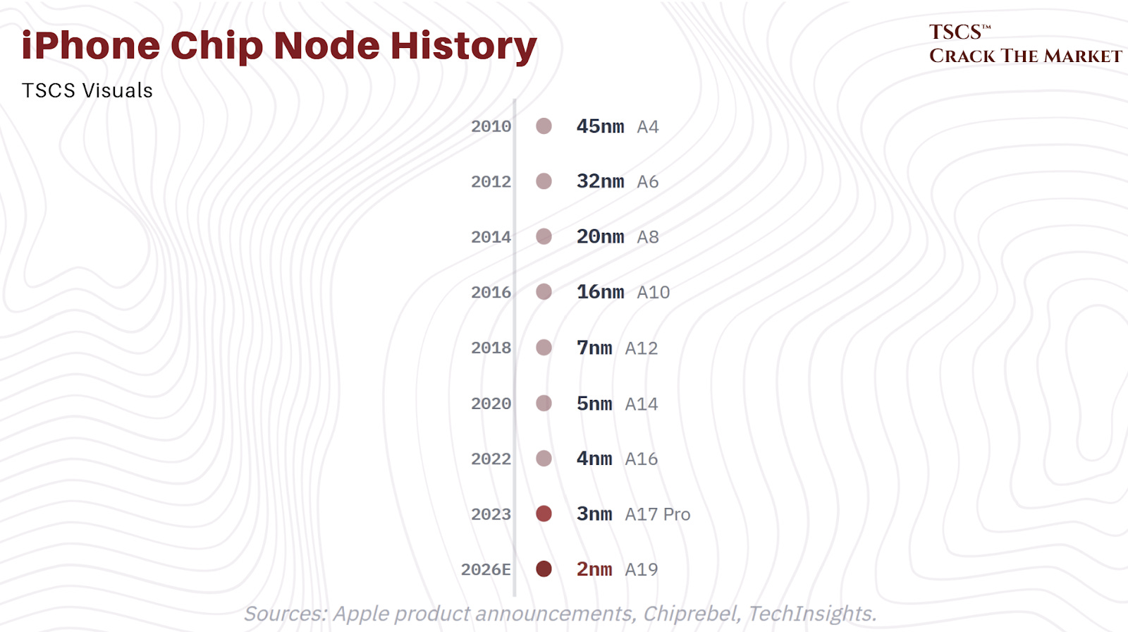
The iPhone’s node history illustrates the cadence perfectly: 45nm in 2010, 20nm in 2014, 7nm in 2019, 3nm in 2023, 2nm in 2026. Each transition requires new tools, new materials, new process recipes. Each new node is 15 to 20% more expensive than the last. The cost to equip a 50,000 wpm fab has escalated from $8 billion at 20nm to $12.5 billion at 7nm to $20 billion at 3nm to $28 billion at 2nm.
And there is a hidden growth engine on top of this: rising ASPs. The price of any lithography generation never falls. ASML’s blended system ASP has compounded at 10 to 15% annually for years. A High-NA EUV tool now exceeds $350 million. The machines get more complex, more productive, and more expensive with each generation, and customers pay because the alternative is falling behind.
Our view: The node transition dynamic is one of those rare cases where the competitive structure of the customer base guarantees demand for the supplier base. Nvidia cannot skip 2nm because AMD will not skip it. Apple cannot skip it because Qualcomm will not. Samsung cannot skip it because TSMC already shipped it. This is a prisoners’ dilemma that resolves in favor of maximum spending every single time. For semicap investors, the question is never “will the next node happen?” It will. The question is “when does the spending intensity peak?” And the answer, given backside power delivery at A16 and the continued stacking complexity of HBM4/5, is: not in this decade. The cost curve is still steepening. We are not near the top.
The China Problem: Why Western Semicap Has Likely Seen Its Best China Quarters
Western semiconductor equipment companies have likely already seen their best China quarters. And the market hasn’t fully priced this in.
China’s wafer fab equipment spending hit a record $49.5 billion in calendar year 2024, representing 42% of global WFE of approximately $118 billion. For 2025, we estimate total WFE reached roughly $120 billion, with China’s share declining to approximately 33% (around $40 billion) as the pre-buy normalizes. That number was not organic demand. It was panic stockpiling ahead of tightening export controls, state-directed capacity buildout on a scale that dwarfs anything the West has attempted, and a strategic pre-buy by companies like Huawei that went from effectively zero WFE spending in 2022 to $7.3 billion in 2024, making it the fourth-largest equipment customer globally. The gap between normal trend spending ($30-35B) and actual 2024 spending ($49.5B) implies roughly $10-15 billion in pull-forward demand that will not repeat.
Every major Western semicap company is now guiding for materially lower China revenue. Meanwhile, Chinese domestic equipment makers are growing 35-50% annually and have already captured an estimated 35% of their home market, beating Beijing’s own interim target. The question is not whether domestic substitution happens, but how fast. The investment thesis here is nuanced but structurally net-negative for Western companies. They can backfill near-term China revenue losses with AI-driven demand from TSMC, Samsung, and the memory players. But the long-term addressable market in China is permanently shrinking. This is the part the consensus 9% WFE CAGR projections tend to gloss over.
The state spending machine
China’s semiconductor ambitions rest on the National IC Industry Investment Fund (the “Big Fund”) across three phases totaling $97 billion in direct capital, with an estimated $150-200 billion mobilized when provincial matching funds and private co-investment are included.
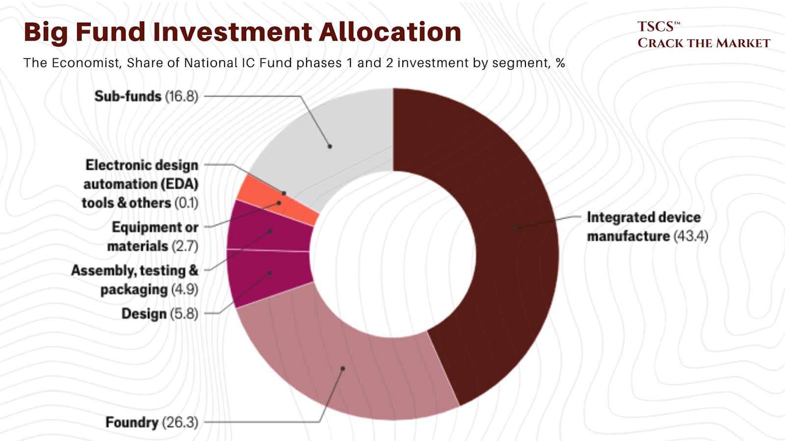
Phase I ($19.6B, 2014-2019) seeded the ecosystem, putting 67% into IC manufacturing and catalyzing the YMTC and SMIC expansions. Phase II ($29.1B, 2019-2024) continued the fab focus but was derailed by a sweeping 2022 anti-corruption purge. Big Fund president Ding Wenwu, Sino IC Capital CEO Lu Jun, and MIIT head Xiao Yaqing all went down. Investment activity froze for five months. Critically, Phase II allocated only RMB 500 million to equipment, a fraction of what ASML alone spends annually on R&D.
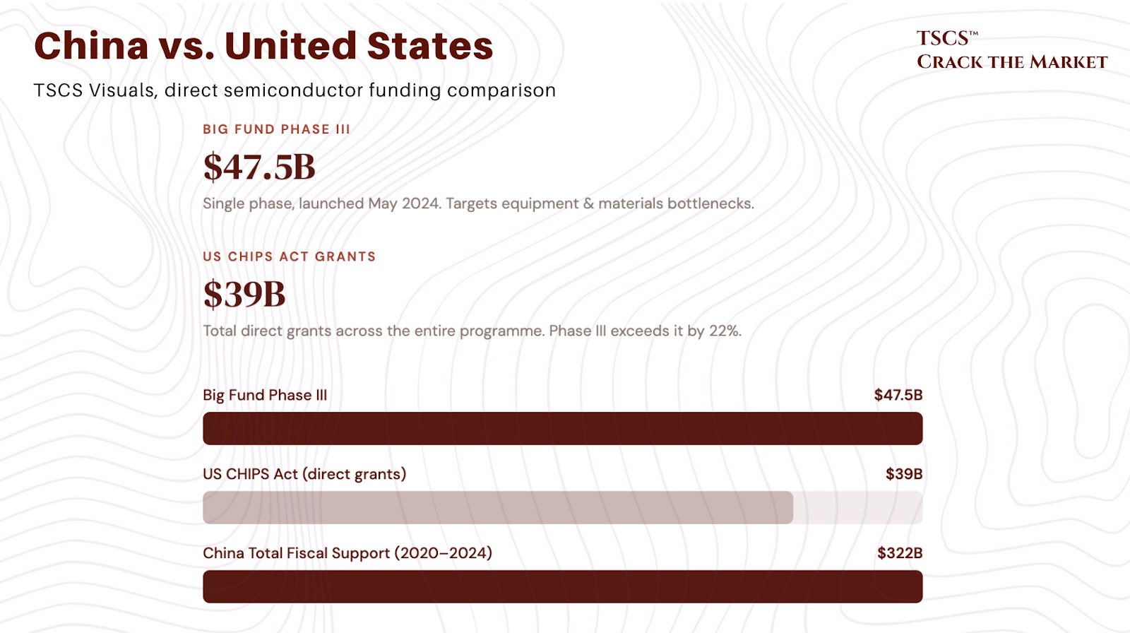
Phase III changed the strategy entirely. Launched in May 2024 at $47.5 billion (larger than Phases I and II combined), it explicitly targets the bottleneck that actually matters: equipment, materials, EDA software, and supply chain components. The fund commenced operations on December 31, 2024, with RMB 93 billion ($12.7B) earmarked for initial investments in materials producers and equipment companies. The strategic logic is unambiguous. Control the tools, and the fabs cannot be held hostage.
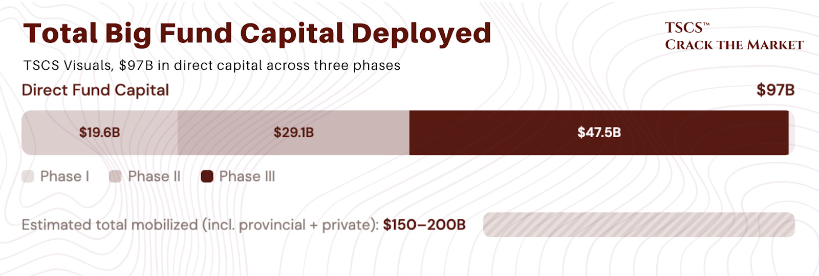
Total Chinese fiscal support for semiconductors from 2020 to 2024 reached an estimated $322 billion when accounting for national IC funds, municipal subsidies, tax preferences, and R&D credits. China’s 2025 central science and technology budget alone is RMB 398 billion ($55B), a 10% year-over-year increase and the third-largest central budget item after defense and debt service. The entire US CHIPS Act provides $39 billion in direct grants. Big Fund Phase III alone exceeds that by 22%. Let that sink in.
SMIC can make 7nm chips, but the economics are brutal
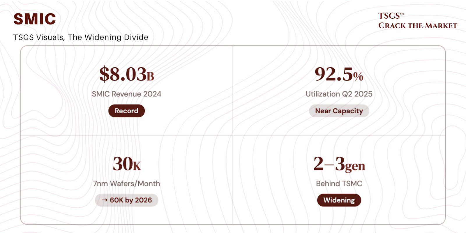
SMIC’s achievement in fabricating functional 7nm chips using multi-patterning DUV lithography was a genuine shock. Confirmed by TechInsights in the Huawei Mate 60 Pro’s Kirin 9000S, SMIC now runs an estimated 30,000 wafers per month at 7nm using ASML’s 1980Di ArF immersion scanners, with capacity scaling toward 60,000 wpm by 2026. Revenue hit a record $8.03 billion in 2024. Utilization reached 92.5% by Q2 2025. Impressive. But the gap with TSMC is widening, not closing.
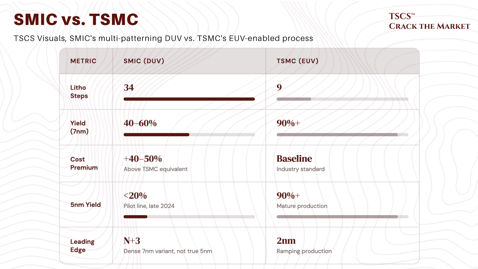
SMIC’s 7nm process requires approximately 34 lithography steps versus 9 with EUV. Costs run 40-50% above TSMC’s equivalent node. Yields are estimated at 40-60%, versus TSMC’s 90%+. At 5nm the picture is far worse: TD Cowen reported yields below 20% on SMIC’s pilot line as of late 2024, and TechInsights confirmed that Huawei’s latest Kirin chip (Mate 80 series) is manufactured on SMIC’s N+3 process, a denser 7nm variant, not true 5nm. TSMC is ramping 2nm production. The technology gap is two to three full generations and multi-patterning DUV becomes exponentially more uneconomical at each subsequent node. You can brute-force 7nm. You can maybe produce something at “5nm” with terrible yields. But the cost-per-transistor curve inverts. This is not a pathway to competitiveness at scale, it is a pathway to strategic capability at enormous cost. Beijing is willing to pay that cost, which is precisely the point. But investors in Western semicap companies should not confuse SMIC’s national security production with commercially competitive manufacturing.
The domestic champions are real
Beyond SMIC, the broader Chinese semiconductor ecosystem has reached an inflection point that investors should not underestimate.
CXMT has emerged as China’s first credible DRAM competitor, producing 16nm DDR5 and LPDDR5X chips and scaling to 280,000-300,000 wafers per month by end 2025. Its global DRAM market share has risen from zero to approximately 6%, with projections of 10-12% by end 2025. The most interesting thing about CXMT is that it is notably still not on the US Entity List, giving it continued access to Western equipment. Both sides recognize this vulnerability. If CXMT gets entity-listed, it hurts Western equipment makers as much as it hurts CXMT.
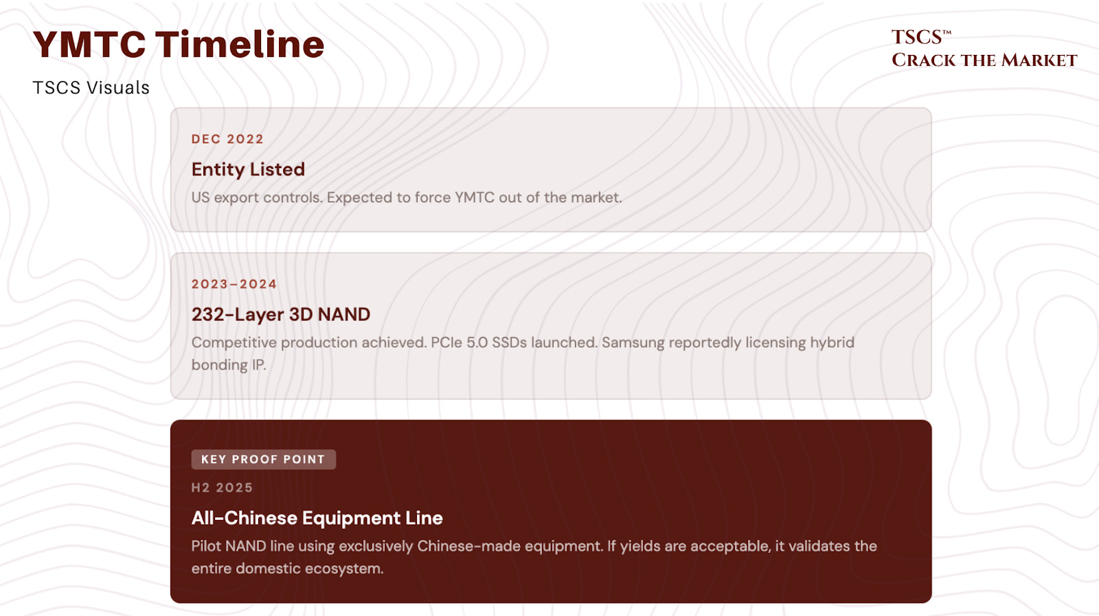
YMTC defied predictions that entity listing in December 2022 would force it out of the market. Instead, it expanded aggressively into domestic NAND, producing competitive 232-layer 3D NAND and launching PCIe 5.0 SSDs. Samsung has reportedly begun licensing YMTC’s hybrid bonding IP for 400-layer NAND, per industry reports from TechInsights and Korean media (independently unverified by TSCS, but widely cited in the semicap analyst community), a remarkable validation from the company that invented flash memory.
YMTC is now building a pilot NAND line using exclusively Chinese-made equipment, expected to begin trial runs in H2 2025. If that line achieves acceptable yields, it validates the entire domestic equipment ecosystem. This is the single most important proof point to watch.
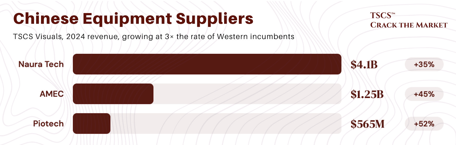
The equipment companies themselves are the most underappreciated part of this story. Naura Technology posted $4.1 billion in 2024 revenue (up 35% YoY), now ranking 6th globally among semiconductor equipment suppliers. It is China’s only platform-type equipment company, covering etch, PVD, CVD, ALD, furnaces, and cleaning. Its etching tools are being tested on SMIC’s 7nm production line. AMEC grew revenue 45% to $1.25 billion, with plasma etching tools verified at the 5nm node and deployed on over 100 production lines worldwide. AMEC’s thin-film deposition revenue surged 1,333% year-over-year in the first nine months of 2025. That is not a typo. Piotech hit $565 million in revenue (up 52%), shipping over 1,000 reaction chambers and building capabilities in CVD, ALD, and hybrid bonding that directly challenge ASM International.
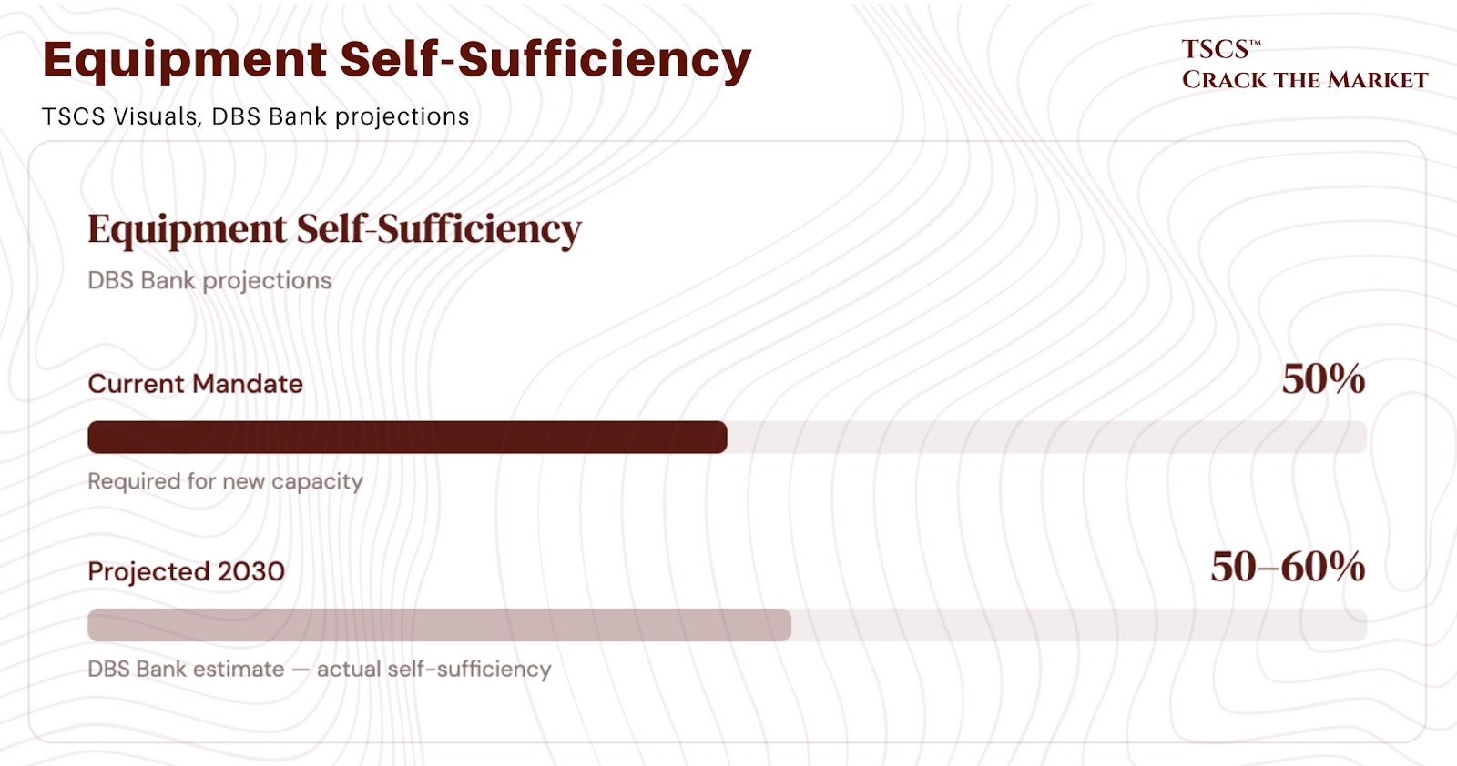
These are companies growing at 3x the rate of Western incumbents, backed by unlimited state capital, operating in a home market where customers are increasingly mandated to buy domestic. The Chinese government now mandates that chipmakers use at least 50% domestic equipment for new capacity additions. DBS Bank projects self-sufficiency reaching 50-60% by 2030.
Where the moats are (and aren’t)
Not all equipment categories are created equal, and this is where the analysis gets interesting from an investment perspective.
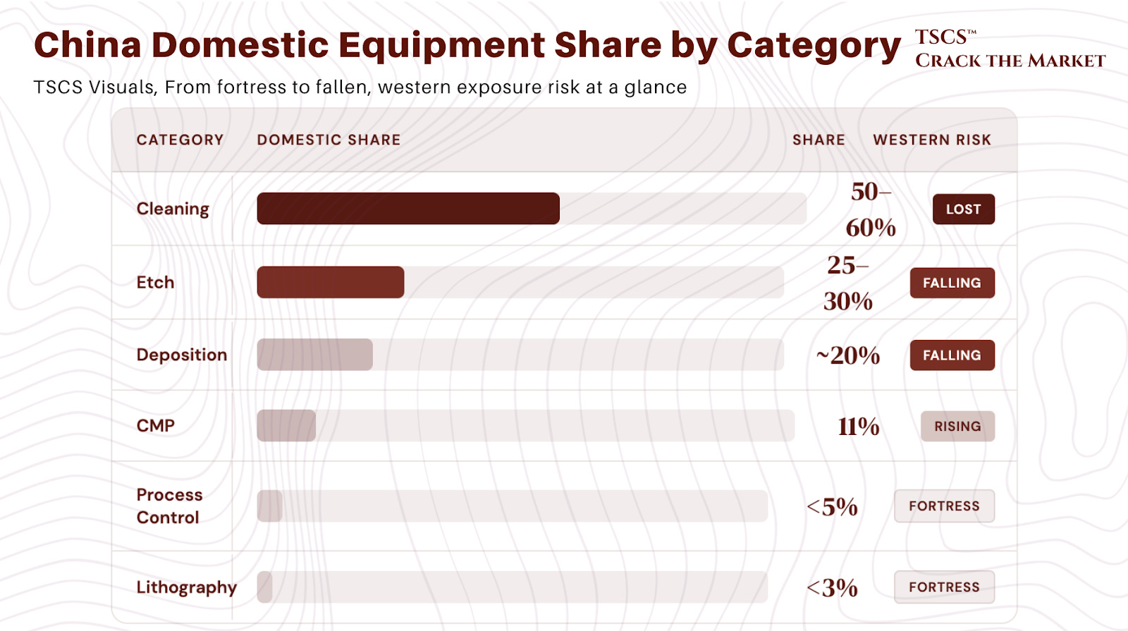
Cleaning is already effectively lost. ACM Research dominates the Chinese market at 50-60% domestic share. Western cleaning revenue in China is most at risk and likely permanently impaired. Etch is falling rapidly, with AMEC and Naura capturing 25-30% domestic share and growing fast. Deposition is on the same trajectory, with AMEC’s thin-film surge as the trend to watch. CMP is a surprising story: Hwatsing drove China’s domestic share from 1.5% to 11% in just two years, directly challenging Applied Materials’ 60% global franchise.
Process control and metrology is the opposite. China’s domestic self-sufficiency is below 5% at advanced nodes, and this is KLA’s moat. The algorithms, yield databases, and optical/e-beam IP represent decades of accumulated advantage. No amount of state capital can shortcut this. As chip complexity rises with AI, process control intensity increases, meaning KLA’s share of WFE has risen from 5.9% to 8.6% over seven years. For investors seeking the most defensible holding through the China transition specifically, KLA is our answer.
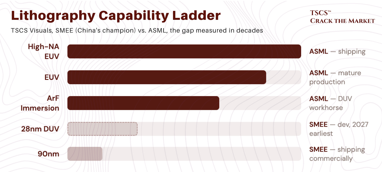
Lithography is the other fortress, but the story is more complicated than most investors appreciate. SMEE (China’s domestic lithography champion) ships commercially at 90nm. A 28nm immersion DUV tool is under development but realistic production insertion is 2027 at earliest. EUV remains, frankly, decades away. This is ASML’s impregnable advantage, but it only protects the EUV franchise. ASML’s DUV business represented roughly 40% of revenue, and China consumed an enormous share of that. ASML generated nearly €20 billion from China in 2024-2025 combined, a figure that includes both DUV systems and a significant number of EUV tools shipped before the latest restrictions took full effect. The “roughly 40% DUV” figure refers to ASML’s global DUV revenue mix; China’s share of DUV specifically was disproportionately high, which is why the combined China revenue figure exceeds what a naive DUV-only calculation would imply. As these dynamics normalize, ASML expects China to fall to roughly 20% of revenue in 2026, per management guidance, with ASML guiding that 2026 total net sales will not be below 2025 levels.
As DUV restrictions tighten and China’s stockpile provides a multi-year buffer reducing reorder demand, ASML’s DUV business will structurally decline. The offset is powerful (EUV demand from AI fabs is surging), but the transition creates a visible multi-year headwind. ASML is a great business in an awkward transition year. The question for ASML is whether the market gives it credit for the 2027-2028 EUV ramp or punishes it for the 2026 China decline.
Export controls keep tightening
The export control landscape has evolved through four major waves. October 2022 restricted equipment for logic below 16nm, NAND above 128 layers, and DRAM below 18nm. October 2023 closed the Nvidia loophole. December 2024 was the most sweeping yet, adding controls on HBM, 24 new equipment types, “node-agnostic” tools targeting multi-patterning techniques, and 140 new Chinese entities.
The Dutch and Japanese have progressively aligned. The Netherlands now requires export licenses for all 193nm immersion DUV scanners, and critically, ASML must now apply for licenses to service, provide spare parts, and issue software updates for previously sold restricted equipment. Japan added restrictions on photoresists and other key materials, with spare parts inventories at Chinese fabs estimated to last only 3-6 months if supply is fully cut.
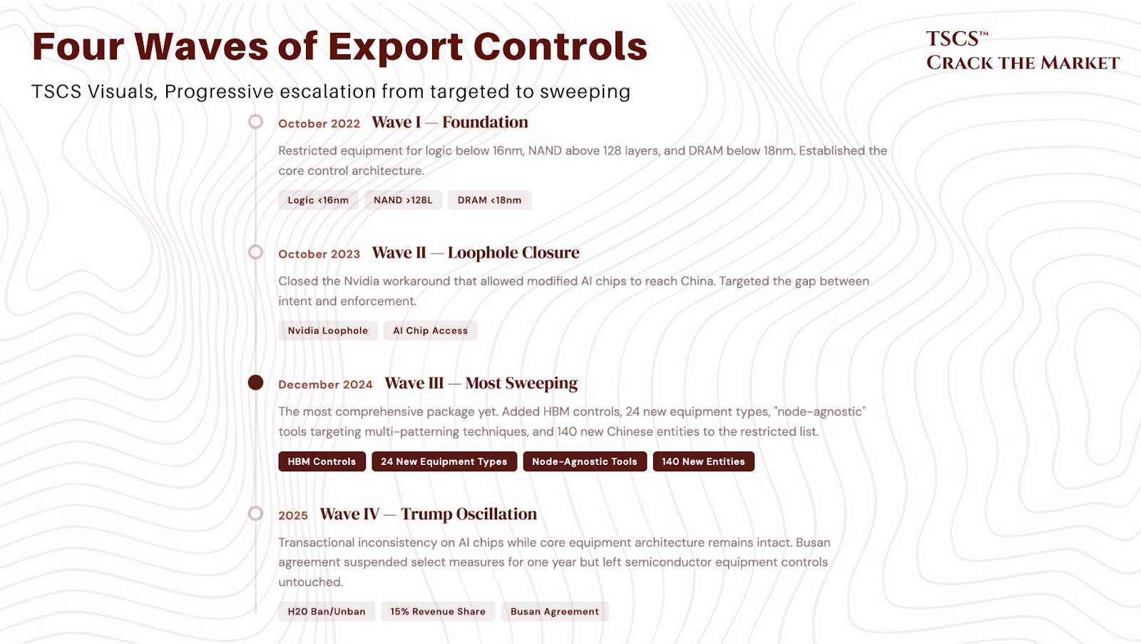
The Trump administration has introduced transactional inconsistency. Banned Nvidia’s H20 in April 2025, reversed the ban in July, then licensed sales with a 15% revenue-sharing arrangement in August. The October 2025 Busan agreement between Trump and Xi suspended the US Affiliates Rule and China’s rare earth export controls for one year, but left all core semiconductor equipment restrictions intact. The fundamental pattern is that the Biden-era control architecture remains in place while the Trump administration oscillates on AI chip access. Congressional hawks on both sides are pushing for codification. De-escalation remains possible but limited. The Busan agreement was a tactical pause, not a strategic reset.
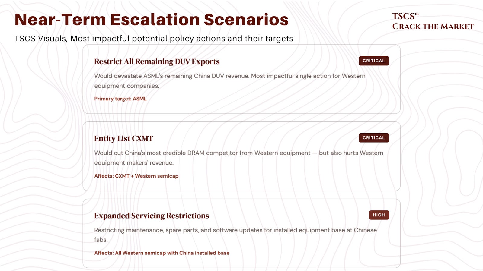
The most impactful near-term escalation scenarios include restriction of all remaining DUV exports (devastating for ASML’s remaining China revenue), entity listing of CXMT, expanded maintenance and servicing restrictions, and mature-node equipment controls. A Section 232 investigation into semiconductor imports is due to report by July 2026.
Peak China is behind us
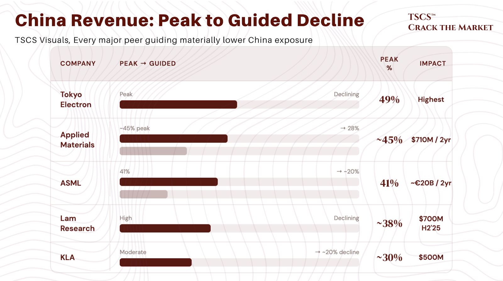
The numbers tell a clear story. ASML went from 41% China revenue to guiding for “significant decline” in 2026, with management calling current levels “in no way normal.” Applied Materials guided for China dropping from roughly 45% at peak quarter to 28% in FY2025, quantifying an export control hit of $710 million over two years. Lam Research guided a $700 million H2 2025 revenue headwind. KLA expects China revenue to decline roughly 20%, with a $500 million impact. Tokyo Electron peaked at 49% China revenue, the highest of any major peer.
The margin impact is disproportionate to the revenue impact, and this is underappreciated. ASML’s CFO confirmed that China revenue is higher margin because it’s overwhelmingly mature DUV tools with fully depreciated R&D. Losing this revenue doesn’t just hit the top line, it hits gross margins by an estimated 100-200 basis points. Applied Materials’ aftermarket services unit hit a record $6.4 billion in FY2025, and service revenue from China is also increasingly at risk as maintenance restrictions expand.
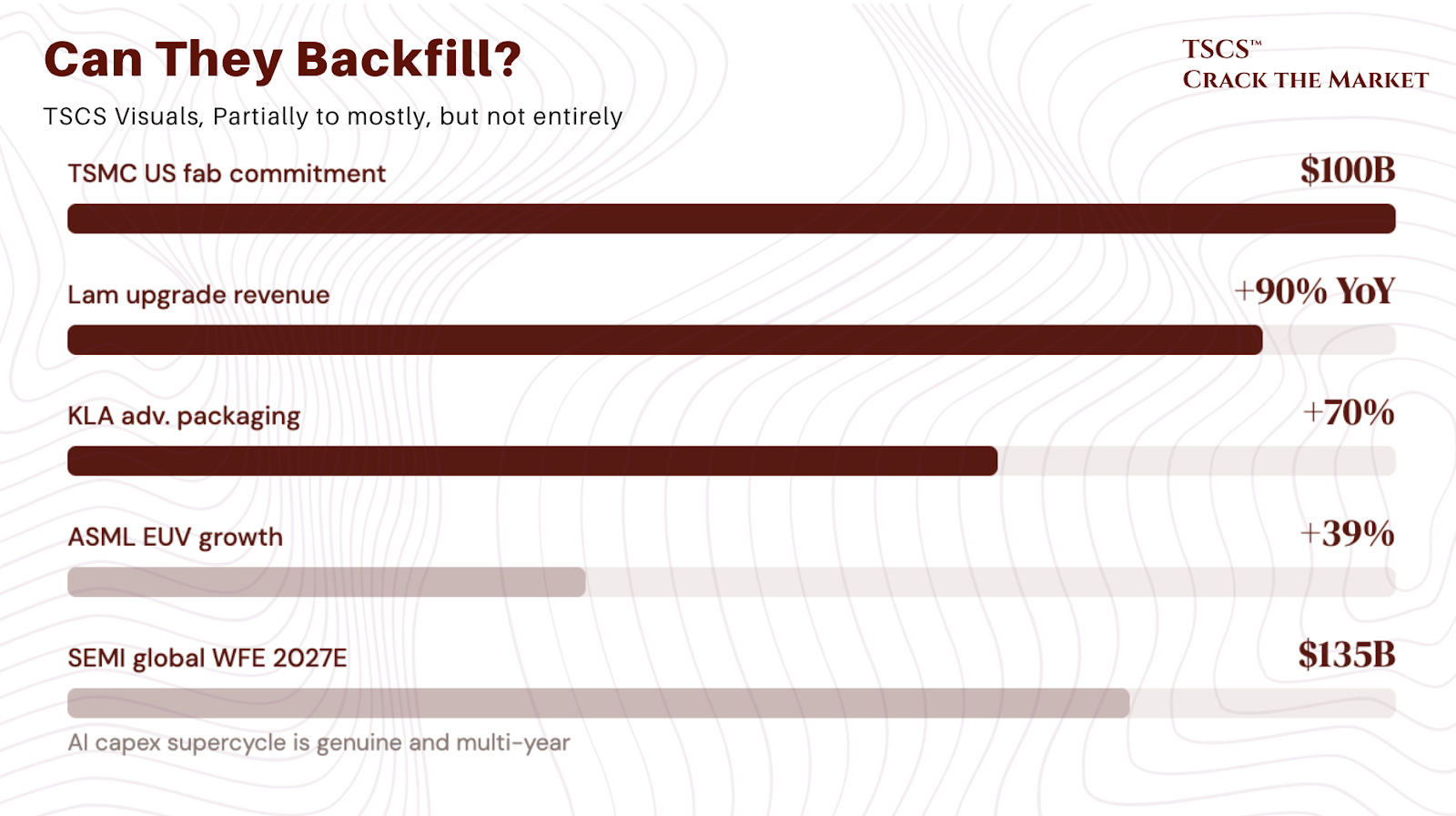
The critical question is whether these companies can backfill. The answer is: partially to mostly, but not entirely. TSMC committed $100 billion to US fabs. The memory supercycle is real. Lam reported upgrade revenue up over 90% YoY. KLA’s advanced packaging revenue is growing 70%. ASML’s EUV business grew 39% in 2025. SEMI projects global WFE reaching $135 billion by 2027. The AI capex supercycle is genuine and multi-year. But it does not fully eliminate the China headwind for companies with the highest exposure and most substitutable products. The backfill works best for companies selling into the leading edge (where China cannot compete) and worst for companies whose China revenue was concentrated in mature-node tools (where domestic substitution is fastest).
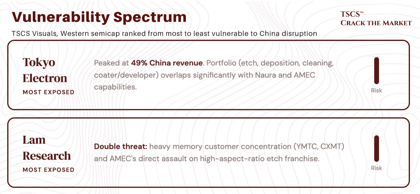
The vulnerability spectrum
Ranking Western semicap companies from most to least vulnerable:
Tokyo Electron and Lam Research are the most exposed. TEL peaked at 49% China revenue with a product portfolio (etch, deposition, cleaning, coater/developer) that overlaps significantly with Naura and AMEC capabilities. Lam faces a double threat: heavy memory customer concentration (YMTC and CXMT were major accounts) and AMEC’s direct assault on its high-aspect-ratio etch franchise. These are the companies exposed to the categories where Chinese substitution is advancing fastest.
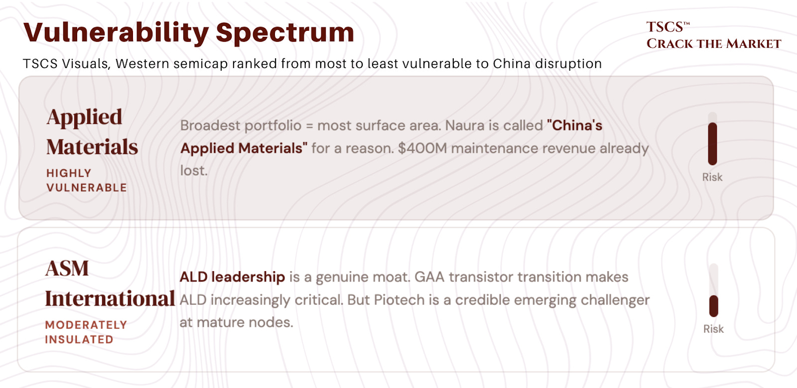
Applied Materials is highly vulnerable for a different reason. The broadest portfolio also means the most surface area for Chinese competition. Naura is often called “China’s Applied Materials” for a reason. AMAT’s management noted that “non-US equipment companies don’t have the same restrictions,” a polite way of saying the US is handicapping its own companies. An estimated $400 million in maintenance services revenue has already been lost.
ASM International is moderately insulated. ALD leadership is a genuine moat, and the GAA transistor transition makes ALD increasingly critical at the leading edge. But Piotech is a credible emerging challenger at mature nodes, having raised 4.6 billion yuan for expansion. The question for ASMi is whether GAA adoption at TSMC and Samsung grows fast enough to offset the inevitable erosion in China.
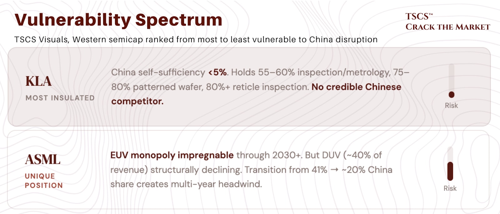
KLA is the most insulated. Process control is the hardest equipment category to replicate. China’s self-sufficiency is below 5% at advanced nodes. KLA holds 55-60% of the total inspection and metrology market, 75-80% of patterned wafer inspection, and 80%+ of reticle inspection. No Chinese competitor has anything remotely credible. KLA also benefits structurally from the same complexity trends driving the AI buildout. This is the closest thing to a “sleep at night” semicap holding through the China transition.
ASML occupies a unique position. The EUV monopoly is impregnable through 2030 and beyond. But DUV immersion represented roughly 40% of revenue, and China consumed an enormous share of that. As DUV restrictions tighten and China’s stockpile reduces reorder demand, ASML’s DUV business will structurally decline. The EUV offset is powerful, but the transition creates a multi-year headwind visible in the guided decline from 41% to 20% China revenue share.
The long view
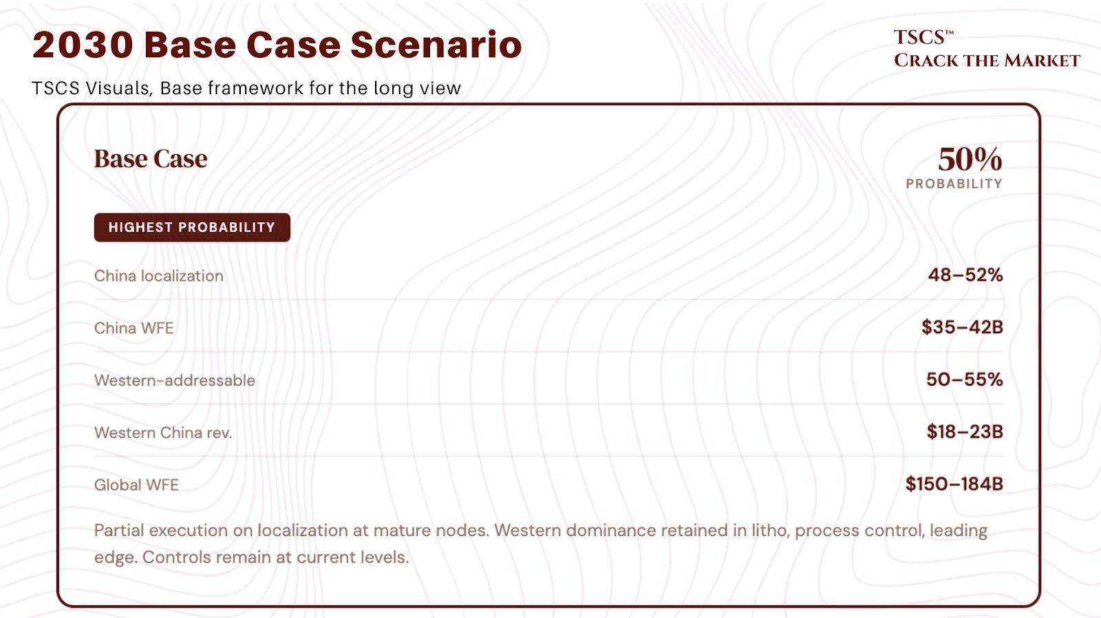
Three scenarios frame the 2030 outlook.
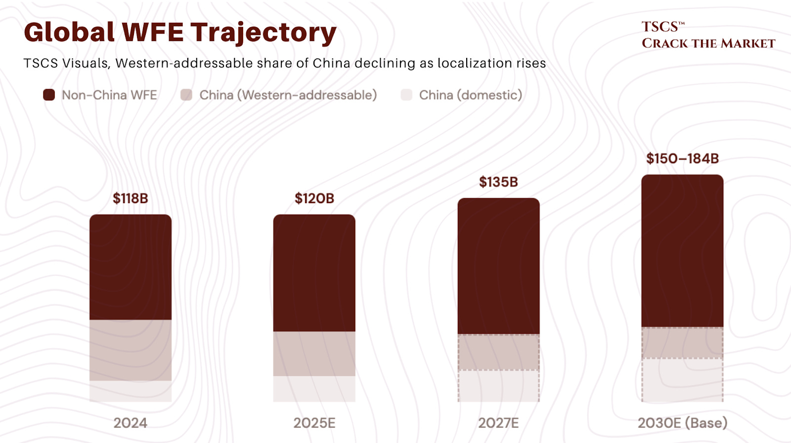
Base case (50% probability): China achieves 48-52% equipment localization, concentrated at mature nodes. Western companies retain dominance in lithography, process control, and leading-edge tools. China WFE spending sustains at $35-42 billion, but the Western-addressable portion declines to 50-55% of that (from roughly 80% today). Western companies’ total China revenue falls from the 2024 peak of $35-38 billion to $18-23 billion, partially offset by AI-driven growth elsewhere. Global WFE reaches $150-184 billion by 2030. We assign this the highest probability because it reflects the historical pattern of Chinese industrial policy: ambitious targets with partial execution, compounded by the persistent difficulty of replicating process control, EUV lithography, and advanced ALD at the leading edge. It also assumes export controls remain roughly at current levels, which is consistent with the Busan framework.
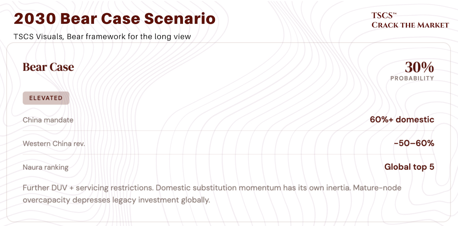
Bear case (30% probability): further DUV and servicing restrictions, China mandates 60%+ domestic sourcing, Naura enters the global top 5 (it is already 6th). Western companies’ China revenue drops 50-60% from peak, and mature-node overcapacity depresses non-China fab investment in legacy nodes. We assign elevated probability because the direction of travel on restrictions is unambiguously tighter, and the momentum of domestic substitution (AMEC’s 1,333% thin-film growth, Naura at $4.1 billion revenue) has its own inertia regardless of trade policy. The constraint on this scenario’s probability is the economic self-harm to Western companies and their governments, which limits Washington’s appetite for full escalation.
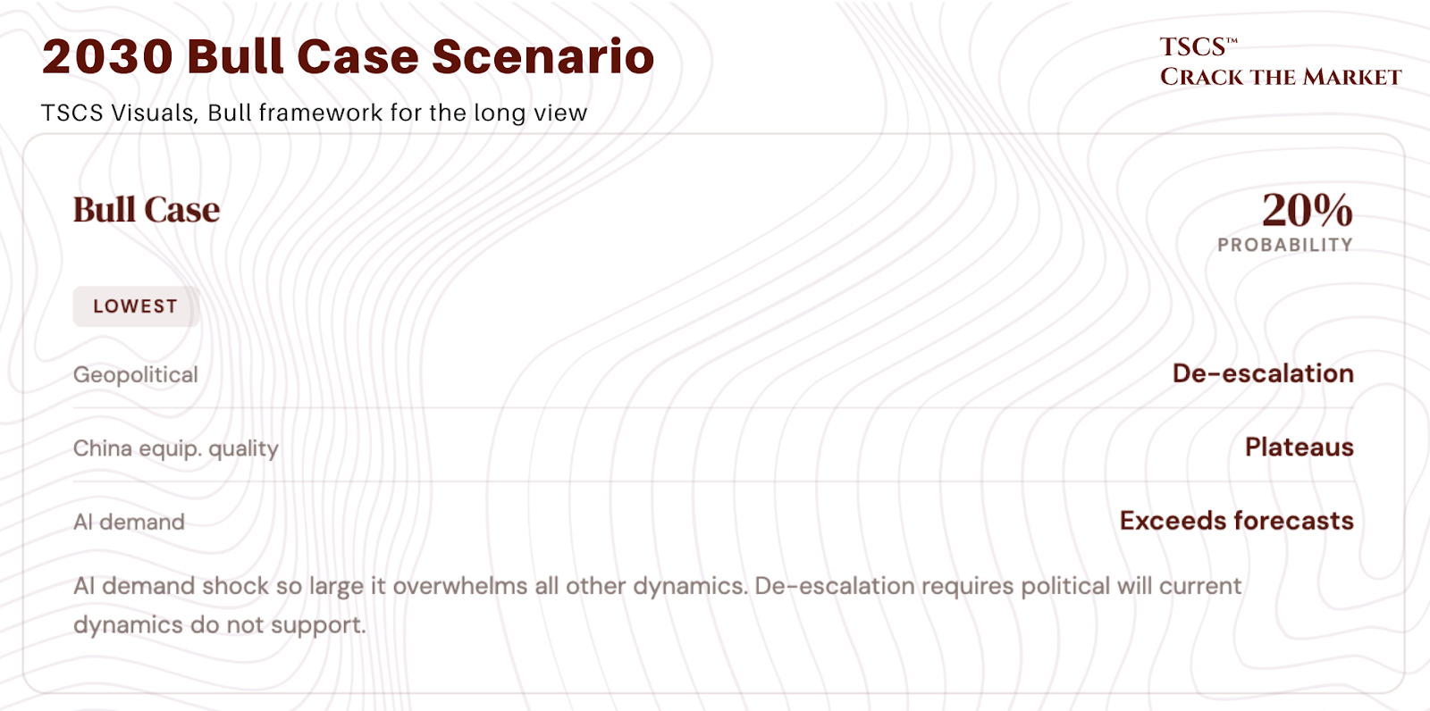
Bull case (20% probability): geopolitical de-escalation loosens some restrictions, Chinese equipment quality plateaus at mature nodes, AI demand exceeds even current forecasts, and total WFE grows fast enough to make the China decline a rounding error. We assign the lowest probability because de-escalation requires political will on both sides that current dynamics do not support, and because Chinese equipment momentum, once achieved, does not simply stop if tariffs ease. The most plausible path to this scenario is an AI demand shock so large that it overwhelms all other dynamics, which is possible but not our base case.
The parallel demand question is critical. Near-term (through 2027), China’s buildout is net additive to global WFE. The capacity is being built for strategic redundancy, not pure market economics, creating demand that wouldn’t exist in a free-market world. But by 2028-2030, cannibalization becomes visible as CXMT floods commodity DRAM markets (targeting 14% capacity share by 2027), YMTC takes 15% of NAND, and Chinese mature-node foundries create persistent overcapacity that pressures UMC, GlobalFoundries, and other non-leading-edge players. The AI capex supercycle is the key variable keeping total WFE expanding despite this dynamic. If AI investment sustains at $150 billion+ annually through the end of the decade, the market absorbs China’s parallel ecosystem. If AI capex disappoints, the overcapacity problem becomes acute.
What to watch
The era of China as a growth engine for Western equipment companies is ending. The composition of China WFE spending is shifting permanently toward domestic suppliers, and export controls ensure that Western companies cannot compete for an increasing share of the market. Chinese equipment self-sufficiency rising from 20% to 50%+ by 2030 means that even if total China spending holds at $35-45 billion, the Western-addressable portion may halve.
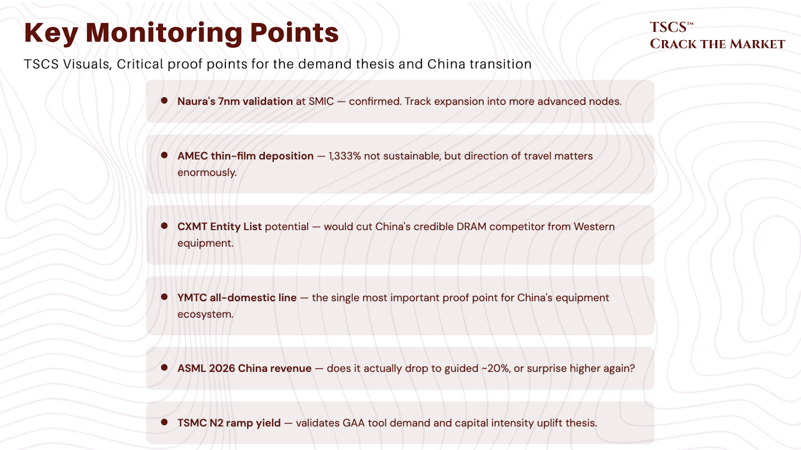
The key things to monitor: Naura’s technology validation at 7nm (confirmed at SMIC), AMEC’s thin-film deposition scaling (1,333% growth is not sustainable but direction matters enormously), CXMT’s potential Entity List addition, YMTC’s all-domestic production line (the single most important proof point for China’s equipment ecosystem), and whether ASML’s 2026 China revenue actually drops to the guided 20% or surprises higher again.
For portfolio positioning, KLA and ASML’s EUV franchise offer the most defensible moats. AMAT, Lam, and TEL carry the most structural risk from domestic substitution. The sector is not uninvestable (global WFE is projected to grow to $135-184 billion by 2030), but the China tailwind that drove 30-45% revenue shares at peak is not coming back. Investors pricing these stocks on a 9% WFE CAGR without adjusting for the mix shift are, in our view, making a mistake.
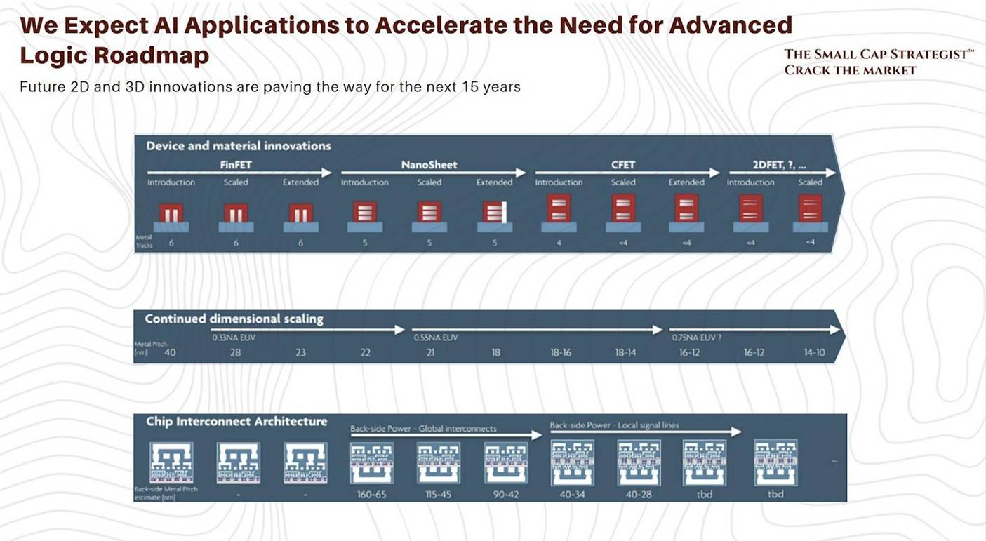
TSMC pushing Moore’s Law further
From supply constraints to demand physics
The China analysis above defines the supply-side constraint on Western semicap growth: a permanently shrinking addressable market in the world’s largest equipment-buying country. Peak China is behind us. Western companies’ aggregate China revenue is on a structural downward trajectory as domestic substitution accelerates and export controls tighten.
But the demand side tells a different, and arguably more powerful, story. The technology roadmap at TSMC and its peers is entering its most equipment-intensive phase in a decade, driven by two simultaneous architectural transitions that have no precedent in the industry’s history: the shift from FinFET to Gate-All-Around transistors at 2nm, and the introduction of backside power delivery at A16. Understanding what these transitions require, what they cost, and which equipment companies they benefit most is essential for assessing whether the structural demand growth can offset the China headwind. The short answer: we believe it can, with margin to spare. Here is why.
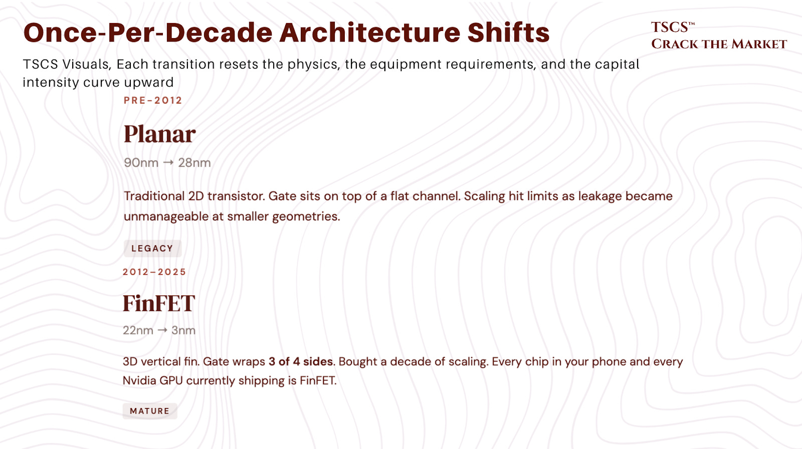
The semiconductor industry changes the architecture of its fundamental building block roughly once per decade. Planar transistors gave way to FinFET in 2012. FinFET is now giving way to Gate-All-Around. Each transition resets the physics, resets the equipment requirements, and resets the capital intensity curve upward. We are in the middle of one of those resets right now.
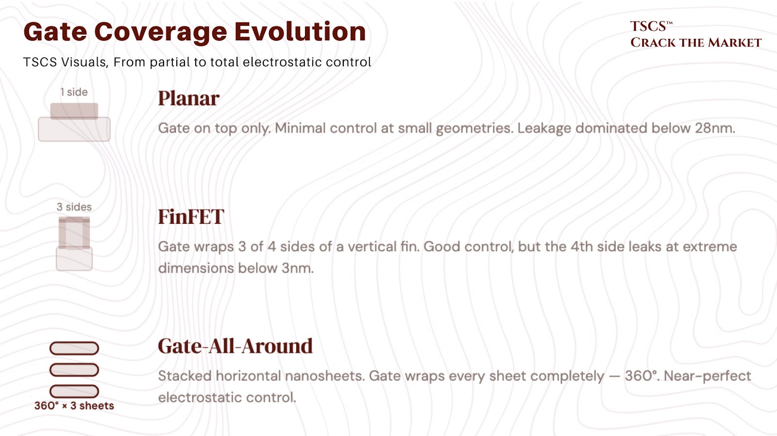
The transistor, for those who need the refresher
A transistor has three parts: a source, a drain, and a gate. Apply voltage to the gate, electrons flow from source to drain. On or off. One or zero. For fifty years, Moore’s Law meant one thing: make the gate smaller. Every 18 months, shrink transistors by half. 90nm in 2003, 65nm in 2005, 45nm in 2007. Each generation was harder than the last, but the industry managed.
Until it stopped managing. At extreme dimensions, electrons refuse to stay where they belong. They leak through insulation, tunnel through barriers, and generate heat in places they should not. The industry bolted on fixes: insulating layers on top, SOI substrates from Soitec to capture electrons below. But the fundamental problem remained. You cannot keep squeezing a 2D structure and expect 3D physics to cooperate.
FinFET bought a decade. GAA buys the next one.
In 2012, the industry introduced FinFET: a 3D transistor architecture where a vertical “fin” of silicon protrudes from the wafer surface and the gate wraps around three of its four sides. Better electrostatic control, less leakage, another decade of scaling. FinFET carried the industry from 22nm through 3nm. Every chip in your phone, your laptop, and every Nvidia GPU currently shipping was built on FinFET.
At 2nm, FinFET hits its wall. The fins become so thin that electrons leak even when the transistor is supposed to be off. The gate controlling three sides is no longer enough when the fourth side is hemorrhaging current.
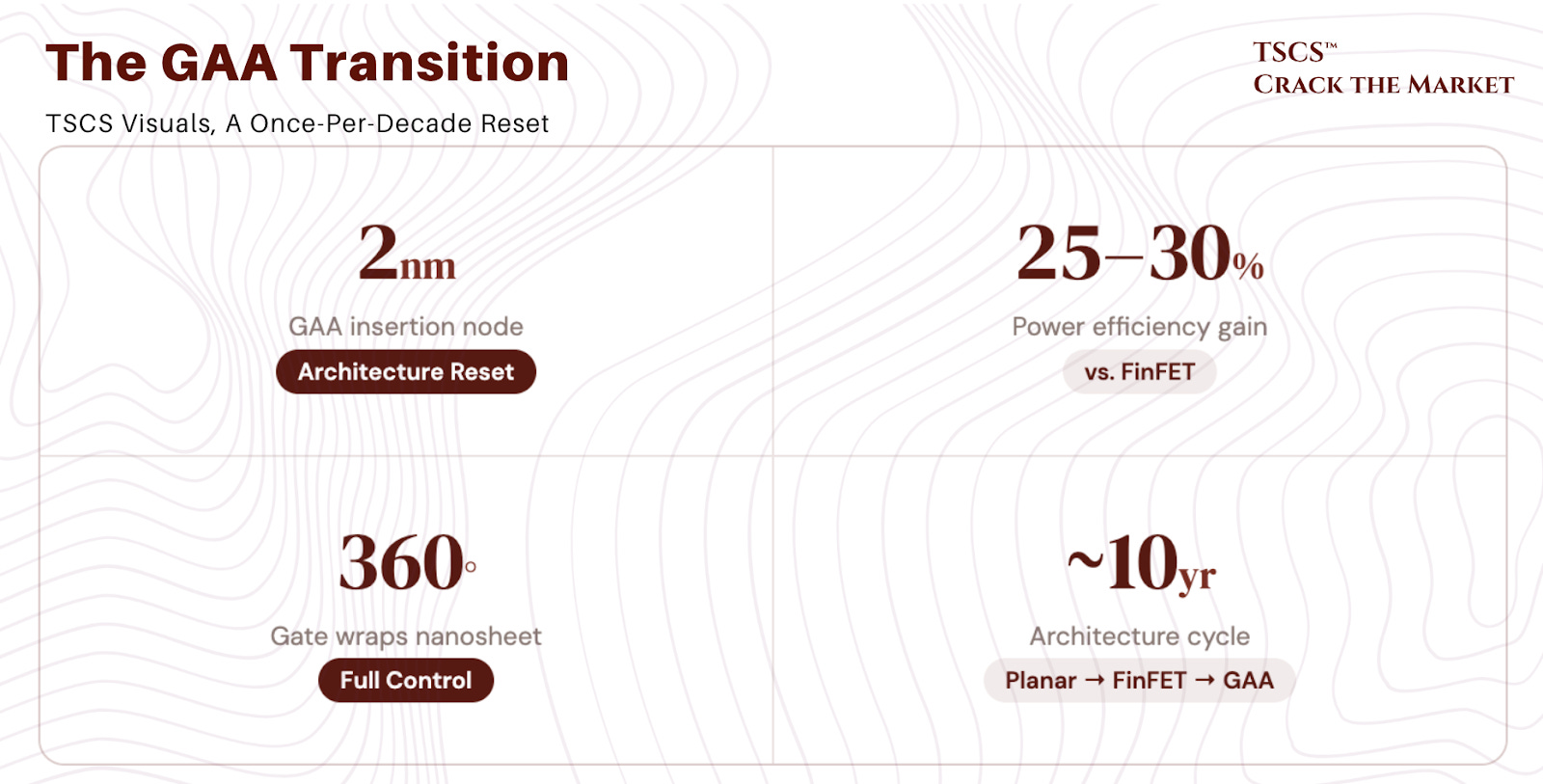
Gate-All-Around replaces the vertical fin with stacked horizontal nanosheets of silicon. The gate wraps completely around each sheet, 360 degrees. Near-perfect electrostatic control. Leakage drops dramatically. Power efficiency improves 25 to 30%. Performance per watt jumps meaningfully. This is not an incremental node shrink. It is a fundamental architectural reset, the kind that happens once per decade and reprices the entire equipment chain.
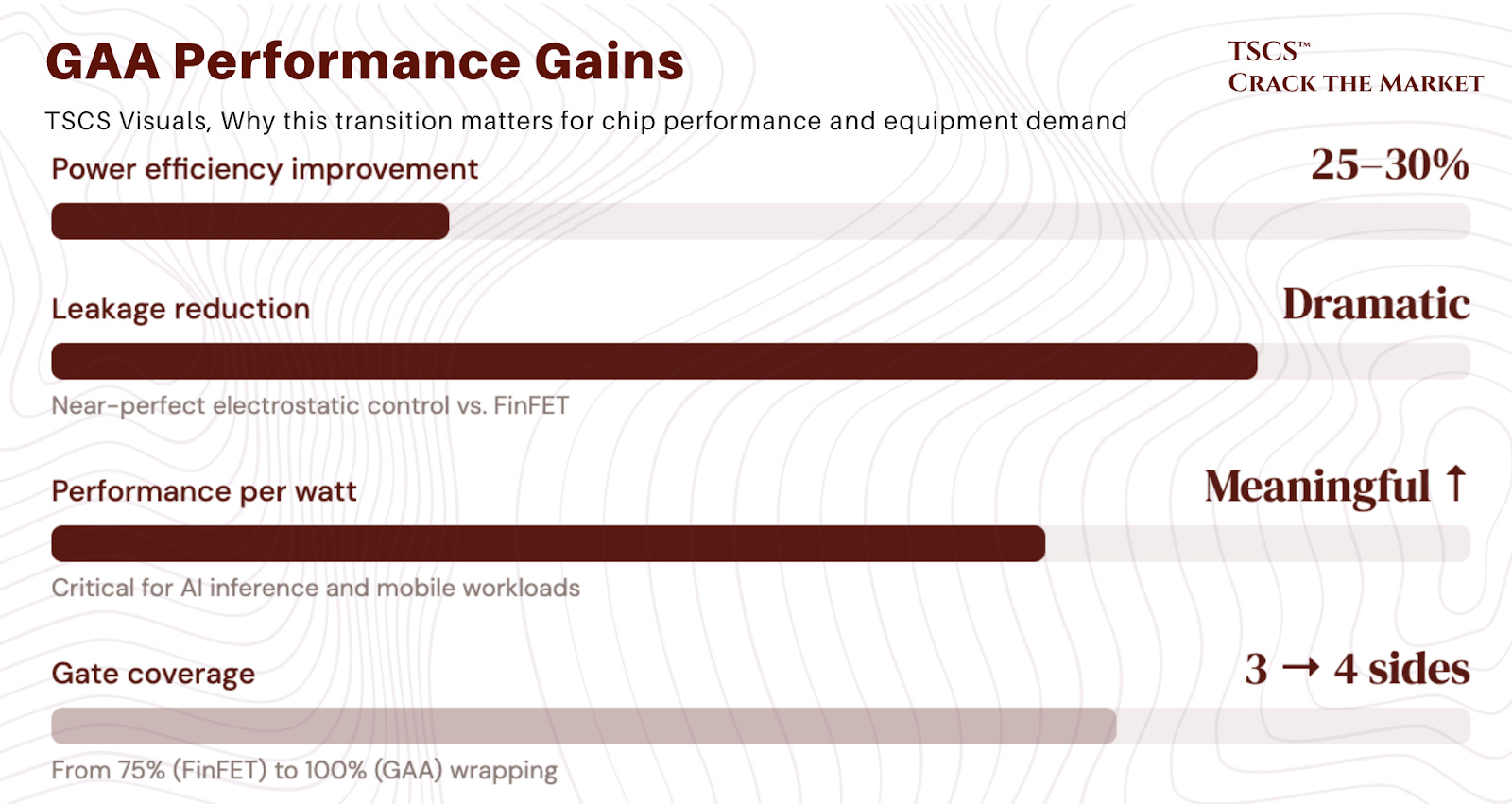
TSCS view: The FinFET-to-GAA transition is, for semicap investors, the most important technology event since EUV insertion at 7nm. Here is why. FinFET nodes (7nm through 3nm) used essentially the same transistor architecture, which allowed 50 to 70% tool reuse between generations. GAA breaks that continuity. New deposition techniques (ASMi’s ALD becomes mandatory, not optional). New etch profiles (Lam and TEL must cut through nanosheet stacks rather than fins). New metrology requirements (KLA must inspect geometries that did not previously exist). New materials. The tool reuse rate at N2 drops substantially, and every percentage point of lost reuse translates directly into incremental equipment purchases. This is why we flagged the tool reuse cliff earlier in this piece. The GAA transition is the mechanism.
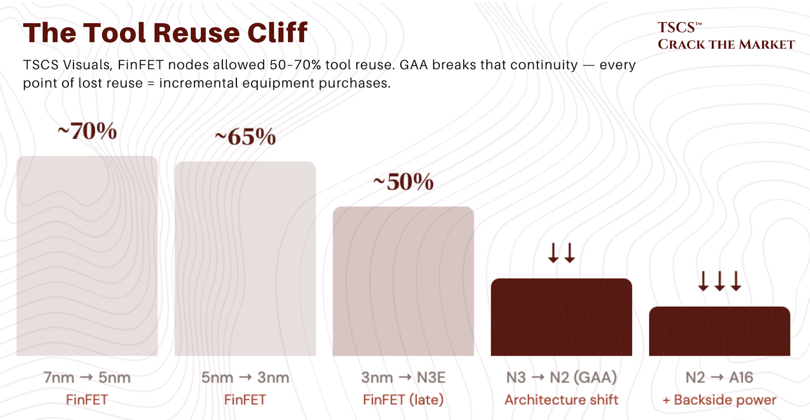
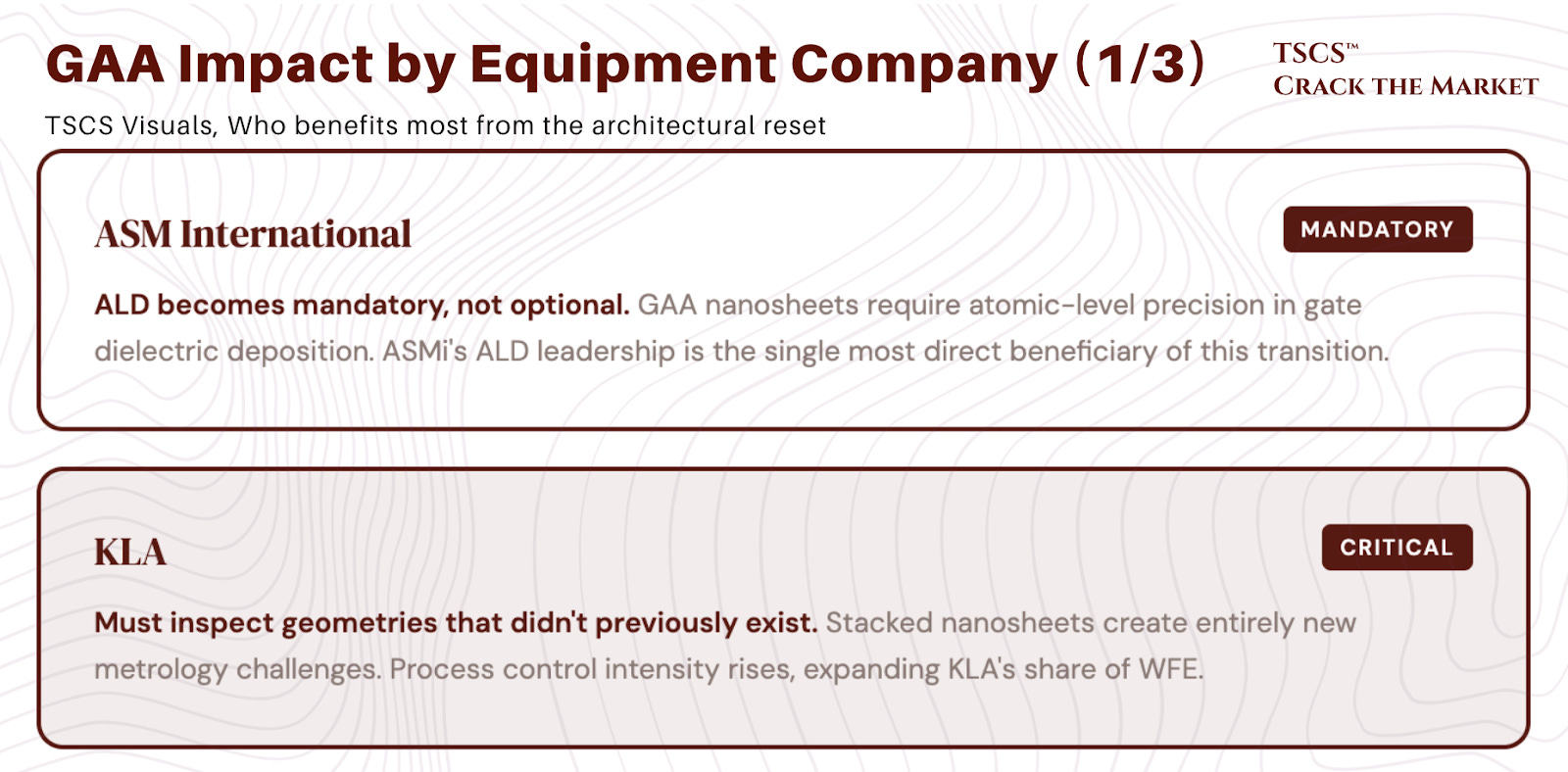
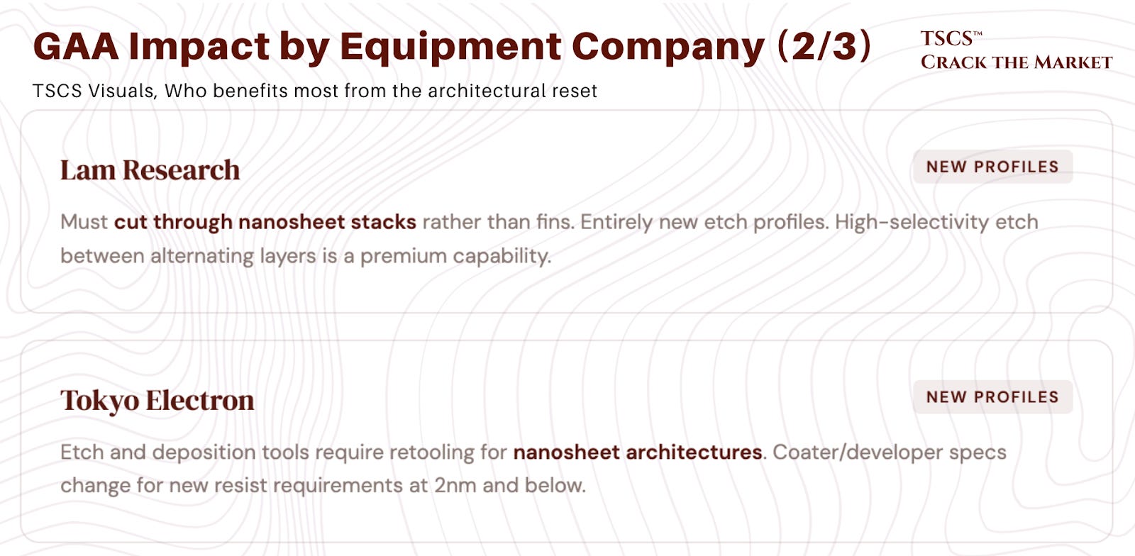
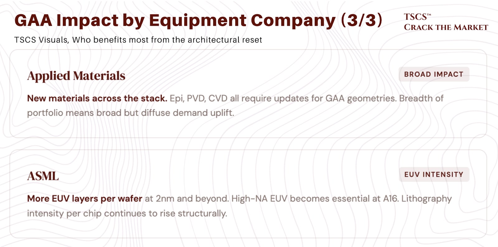
N2: the node that matters more than any in a decade
N2 is not just another step down the roadmap. It is viewed as a large and long-lasting node, analogous to what 28nm was for mature applications or what 7nm was for the EUV era. The power efficiency gains (25 to 30%) make it essential for data centers that are operating against hard thermal and electrical limits. Hyperscalers are not adopting N2 because it is new. They are adopting it because their power bills demand it.
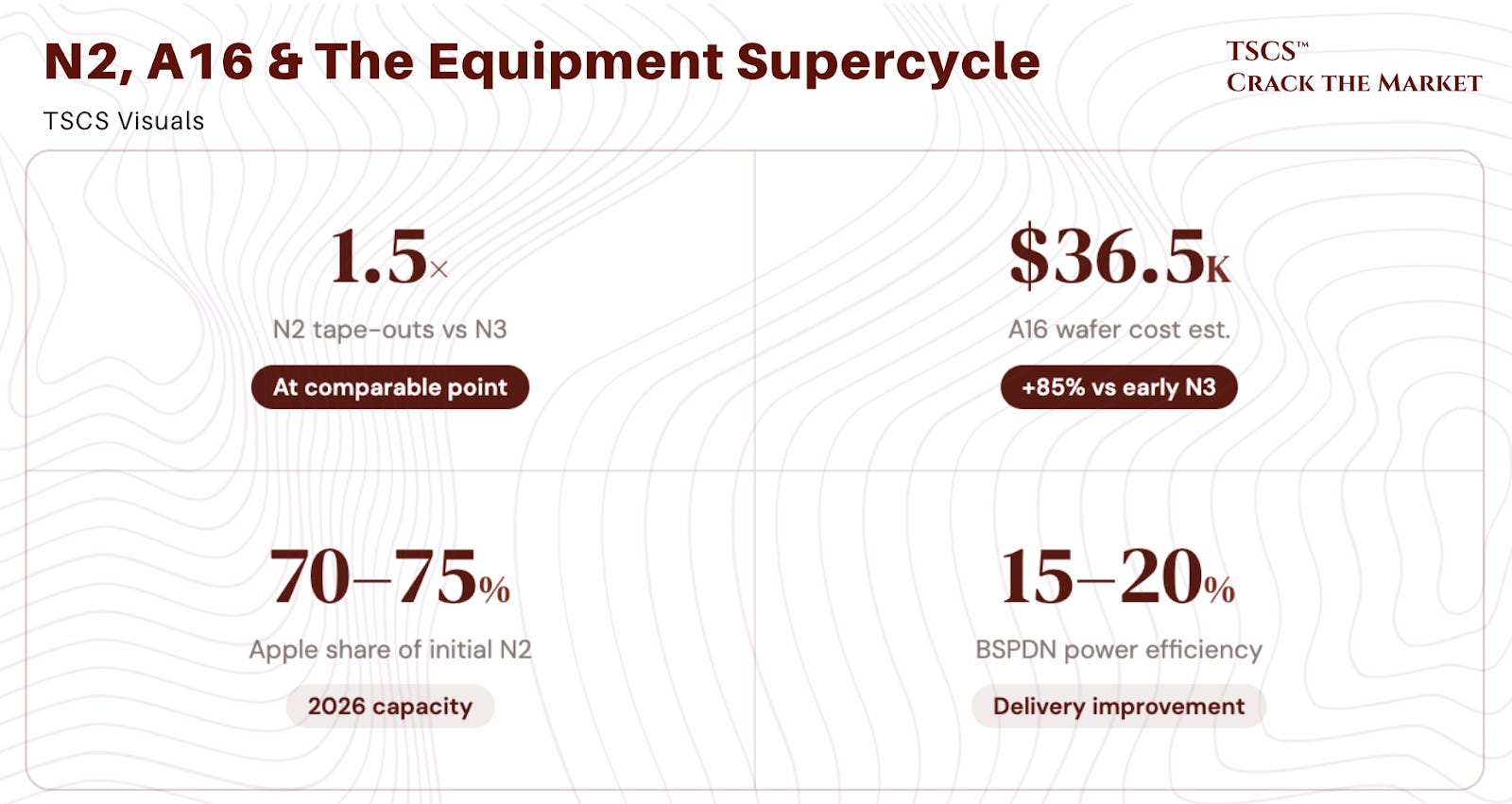
Demand confirms this. N2 tape-outs are running 1.5x higher than N3 at comparable lifecycle points, despite higher cost and complexity. Apple is expected to absorb 70 to 75% of initial N2 capacity in 2026, with AMD and other HPC customers following. TSMC is building N2 capacity knowing it will be fully utilized before the first wafer ships.
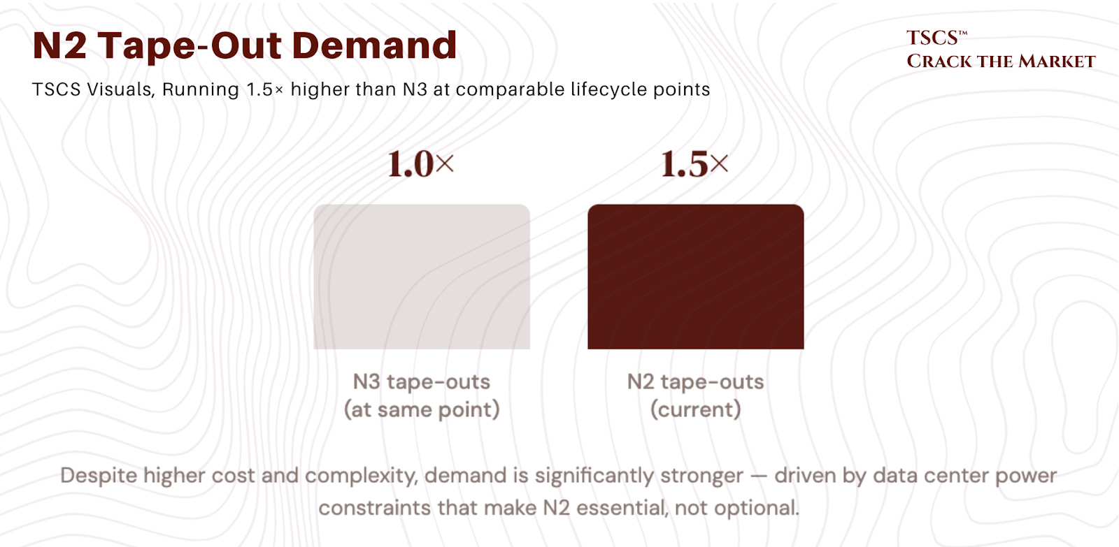
A16 and backside power delivery: rewiring the skyscraper from underneath
Beyond N2, TSMC’s A16 process (1.6nm class) introduces backside power delivery (BSPDN), branded as Super Power Rail. This is the second architectural breakthrough in two node generations, which is unprecedented.
The concept requires understanding chip geometry. A modern chip is a vertical structure: transistors at the base, 15 to 20 metal wiring layers stacked above, routing both data signals and power delivery from the top down. As chips get denser, this creates congestion. Power and data compete for the same routing channels, generating resistance, voltage loss, heat, and electrical noise.
Backside power delivery separates the two entirely. Power enters from the back of the wafer, routed directly to transistors through the silicon substrate. Data signals stay on the front. Power and data never share the same pathways. The result is lower resistance, cleaner signals, less heat, and higher transistor density because the front-side metal layers are freed up exclusively for data routing.
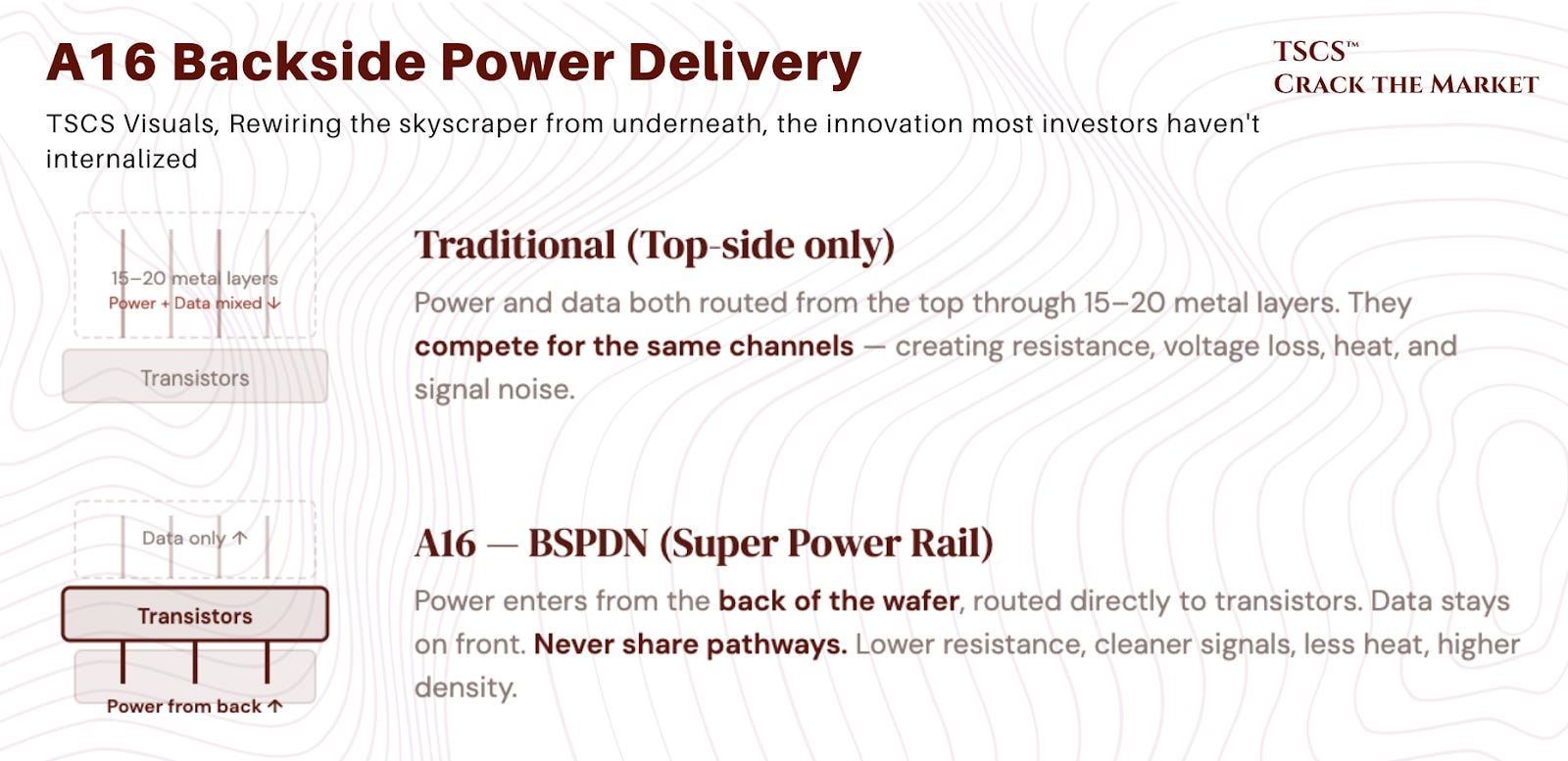
The engineering is extreme. Wafers must be thinned to near invisibility and aligned with atomic precision on both sides. A single A16 wafer is estimated to cost roughly $36,500, an 85% premium over early N3. Customers will pay it without hesitation. For a hyperscaler spending billions annually on electricity, a 15 to 20% improvement in power delivery efficiency pays back the wafer premium thousands of times over across a fleet of millions of chips.
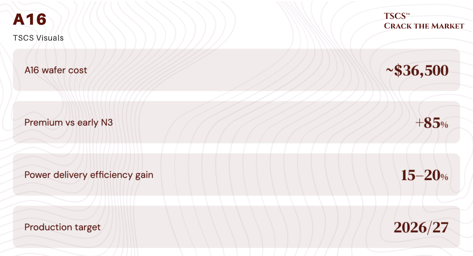
Our view: Backside power delivery is the innovation that most generalist investors have not yet internalized, and it has profound implications for the equipment chain. BSPDN requires processing both sides of the wafer, which effectively doubles the number of equipment steps for the power delivery layers. Wafer thinning and backside alignment require entirely new tool sets (grinding from Disco, bonding from Besi, new deposition and etch steps from AMAT and Lam). This is not theoretical future demand. TSMC’s A16 is on the roadmap for 2026/2027 production, and equipment orders for the pilot lines are already flowing. If GAA at N2 is the tool reuse cliff, BSPDN at A16 is the tool count expansion. Together, they represent a one-two punch of equipment intensity escalation that the 9% WFE CAGR consensus may be underestimating. The semicap companies most levered to this dynamic are ASMi (ALD for GAA), Disco (wafer thinning for BSPDN), AMAT (materials engineering for both), and KLA (inspection complexity doubles when you process both sides of a wafer).
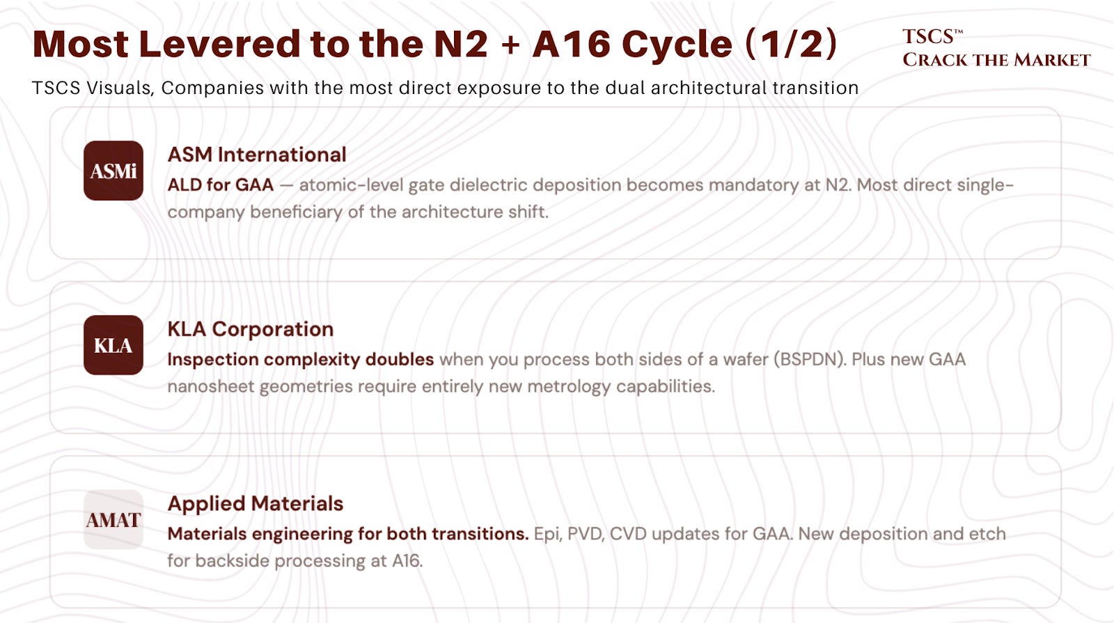
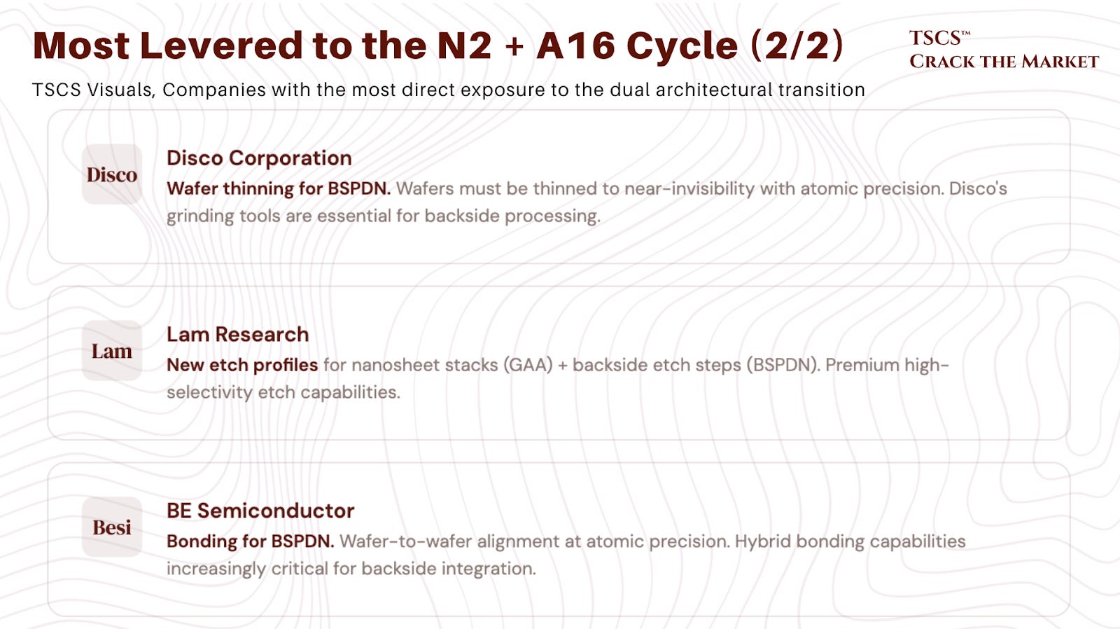
The roadmap has visibility through the 2030s
What makes the semiconductor industry unusual among capital goods sectors is that the technology roadmap provides genuine multi-year visibility. GAA at 2nm is here. Backside power delivery at A16 is next. Beyond that, TSMC’s roadmap extends through A14 and beyond, with each node requiring further equipment innovation. CFET (complementary FET, stacking NMOS on top of PMOS) is the next architectural transition after GAA, likely arriving in the early 2030s. High-NA EUV from ASML is ramping now and will be the workhorse lithography tool for sub-2nm nodes.
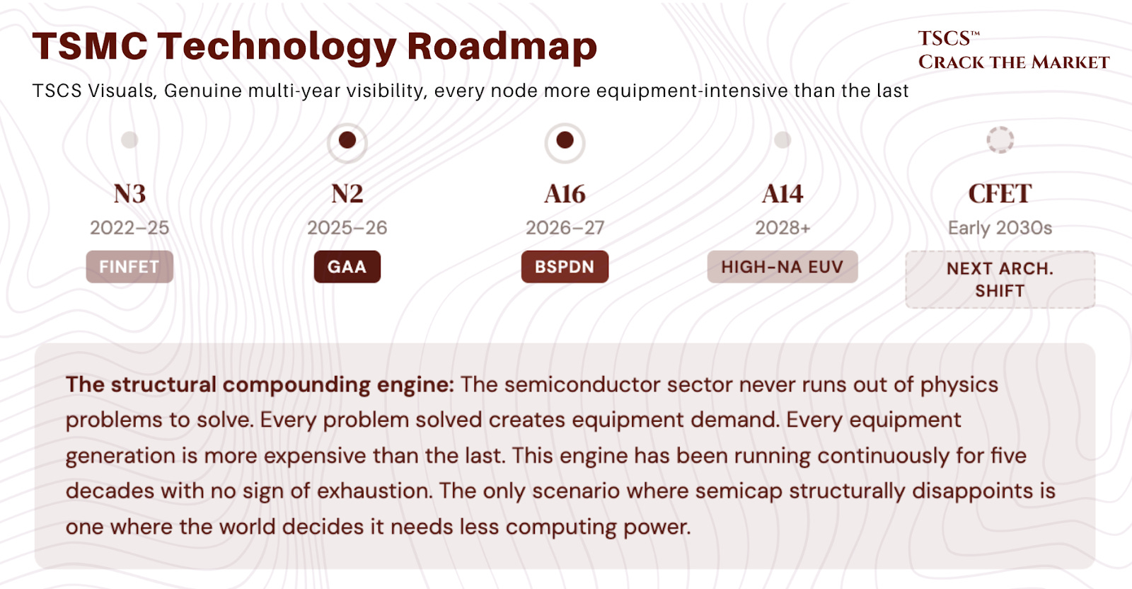
The semiconductor sector never runs out of physics problems to solve. Every problem solved creates equipment demand. Every equipment generation is more expensive than the last. This is the structural compounding engine underneath the semicap investment thesis, and it has been operating continuously for five decades with no sign of exhaustion.
TSCS view: We want to be direct about something. The visibility on this roadmap is real, but it is not the same as certainty. CFET is a laboratory concept, not a production technology. High-NA EUV has shipped fewer than a dozen systems. The history of semiconductor manufacturing is littered with technologies that worked in the lab and failed in the fab (450mm wafers, anyone?). What gives us confidence is not that every roadmap milestone will hit on schedule, but that the direction of travel is unambiguous: more complexity, more equipment intensity, more spending per node. Even if A16 slips by a year or CFET arrives late, the secular trend of rising WFE per unit of computing capacity is not reversing. The only scenario where semicap growth structurally disappoints is one where the world decides it needs less computing power. We do not see that scenario on any reasonable horizon.
The back-end revolution: advanced packaging and the real AI bottleneck
For decades, the back end of semiconductor manufacturing was the unglamorous cousin. Slice the wafer, bond some wires, encase it in plastic, test it, ship it. Labor-intensive work done in Malaysia and the Philippines by OSATs (outsourced assembly and test companies) like ASE and Amkor operating on thin margins. Nobody wrote research reports about packaging.
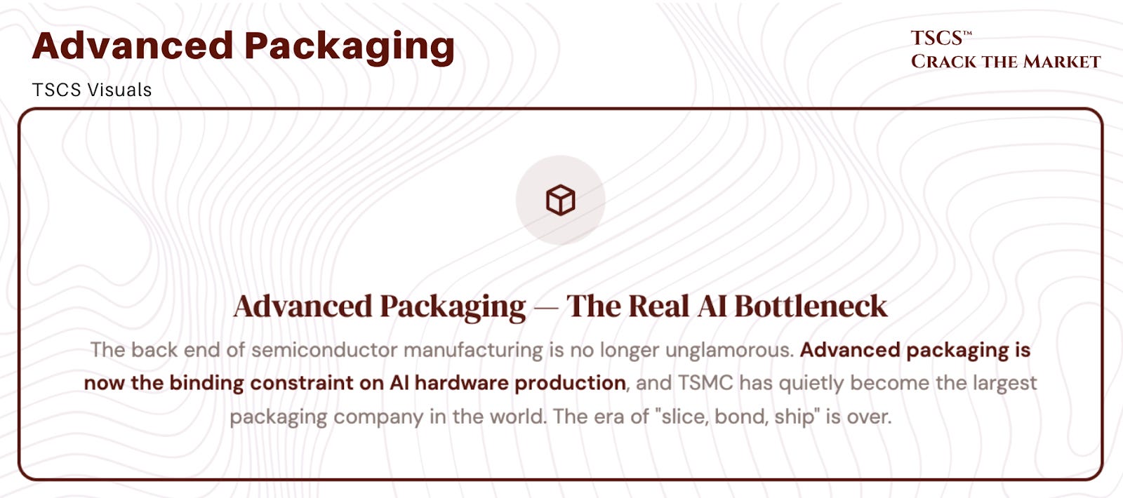
That era is over. Advanced packaging is now the binding constraint on AI hardware production, and TSMC has quietly become the largest packaging company in the world.
Why packaging became the bottleneck
The era of the single monolithic chip is effectively finished. EUV lithography can only project a finite field of view (roughly 858 square millimeters, the reticle limit), meaning it is physically impossible to print a chip larger than that in one shot. Modern AI accelerators demand computational brains that exceed this limit. Nvidia’s Blackwell is not one chip. It is multiple chiplets stitched together into a single system.
The solution is not a bigger chip. It is better packaging. Instead of one massive die, designers create multiple smaller dies that fit within lithography constraints and integrate them on a shared substrate. Performance gains now come from how chips are assembled, not just how small the transistors are.
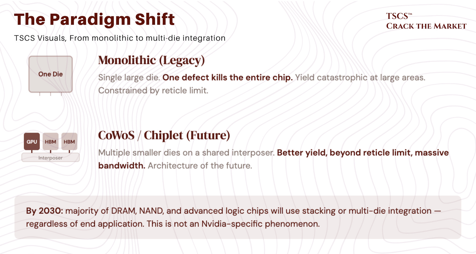
This shift also solves a second problem: yield. A large monolithic die suffers catastrophic yield loss because one defect kills the entire chip. Smaller chiplets improve manufacturing efficiency dramatically. Defective chiplets get discarded individually while functional ones are assembled into complete systems. Better economics, faster scaling, and a path around the reticle limit. Chiplets are not a compromise. They are the architecture of the future.
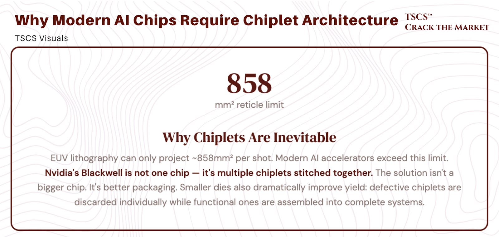
TSCS view: The chiplet transition is the single most underappreciated structural shift in semiconductors today, and most investors are still framing it as an Nvidia-specific phenomenon. It is not. By 2030, the majority of DRAM, NAND, and advanced logic chips (including smartphone processors) will use some form of stacking or multi-die integration regardless of the end application. The number of wafers employing stacking technologies is projected to rise from 500,000 wpm (7% of total consumption) in 2025 to 3.5 million wpm (over 35%) by 2030. That is a 7x increase in five years. The back-end equipment companies serving this transition (Besi for bonding, Disco for grinding, Advantest for testing) are not riding a cycle. They are riding a structural replatforming of how the entire industry assembles its products.
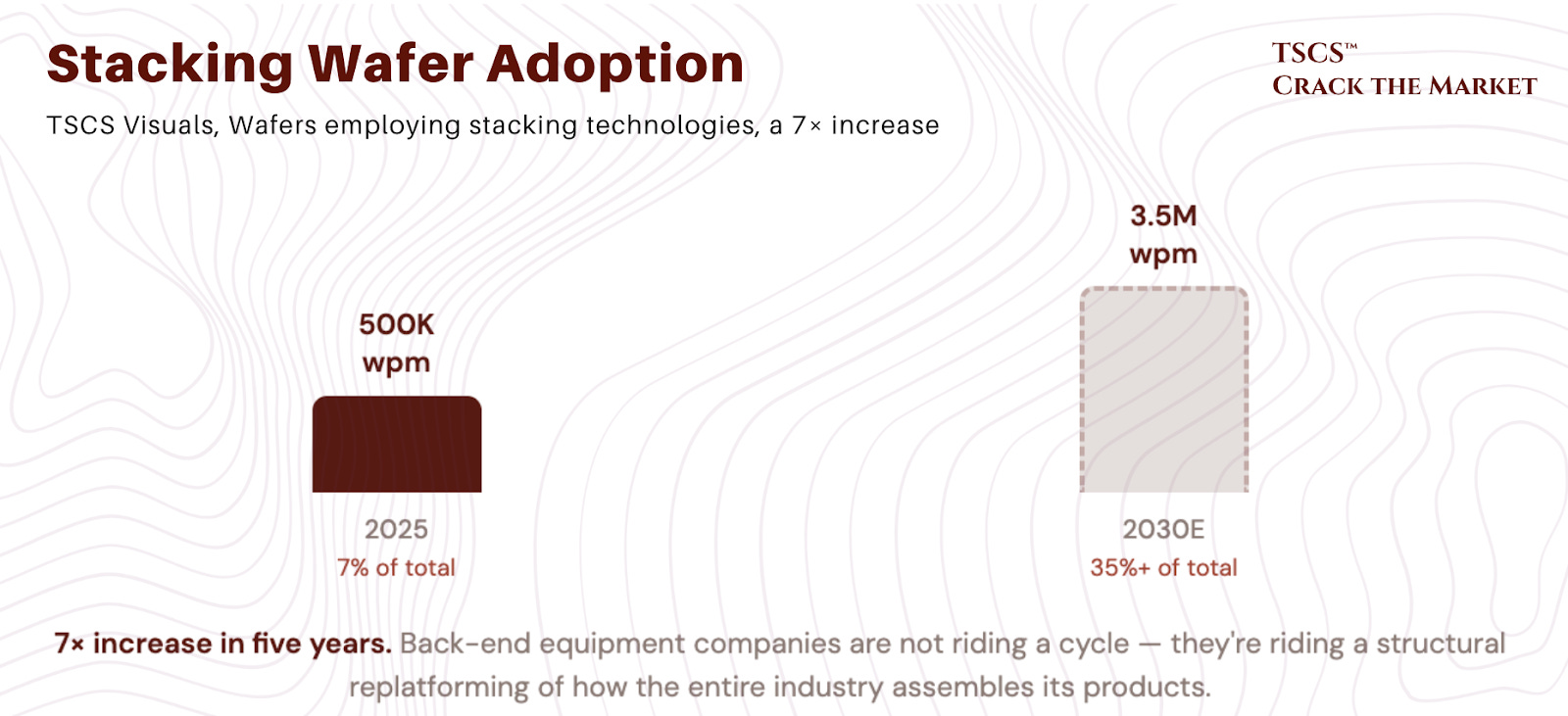
CoWoS: the three letters holding back AI scaling
CoWoS (Chip-on-Wafer-on-Substrate) is TSMC’s 2.5D packaging technology, and it is the chokepoint of the global AI supply chain. Multiple logic and memory dies are placed side by side on a silicon interposer, connected by ultra-dense wiring that enables massive bandwidth between compute and memory. Instead of chips shouting at each other across a circuit board, they whisper across microns of silicon.
This matters because AI accelerators are memory-bandwidth limited, not compute limited. The GPU can crunch numbers faster than the memory can feed it data. CoWoS solves this by putting HBM stacks directly adjacent to the logic die on a shared interposer, slashing latency and multiplying bandwidth. Every Nvidia GPU from Hopper through Blackwell through Rubin ships on CoWoS. Every major custom ASIC from Google, Amazon, and Microsoft uses it or something functionally equivalent.
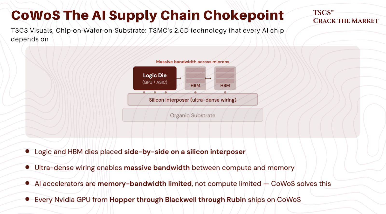
TSMC controls roughly 90% of global CoWoS capacity. Past shortages of Nvidia GPUs were not caused by logic fabrication bottlenecks. They were caused by insufficient CoWoS packaging capacity. TSMC is investing aggressively, targeting over 140,000 CoWoS-equivalent wafers per month by 2027 with entire factories dedicated solely to this step. But demand is growing faster than capacity, which is why CoWoS remains the binding constraint on AI chip supply.
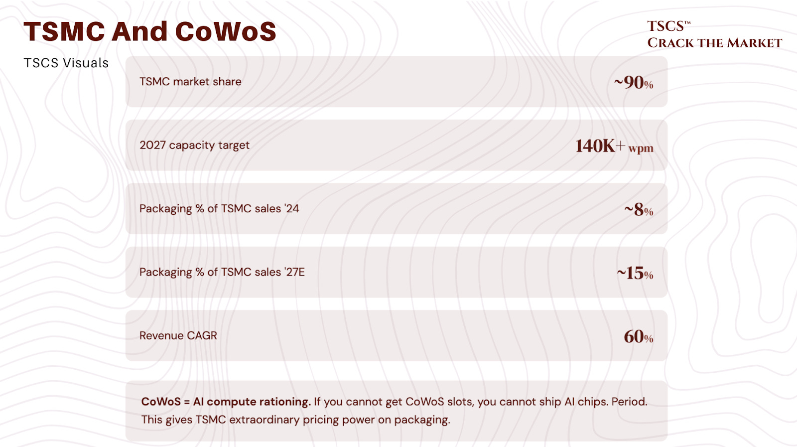
TSCS view: CoWoS capacity allocation is, in practice, how TSMC rations access to AI compute. If you cannot get CoWoS slots, you cannot ship AI chips. Period. This gives TSMC extraordinary pricing power on packaging, which is showing up in the numbers: advanced packaging revenue expanding at a 60% CAGR from 8% of sales in 2024 to an estimated 15% by 2027. The investment implication is that back-end equipment is no longer a secondary consideration. It is a primary growth driver. The companies supplying tools into TSMC’s CoWoS expansion (deposition, lithography for interposers, bonding, grinding, testing) are seeing order growth that rivals or exceeds the front-end equipment cycle.
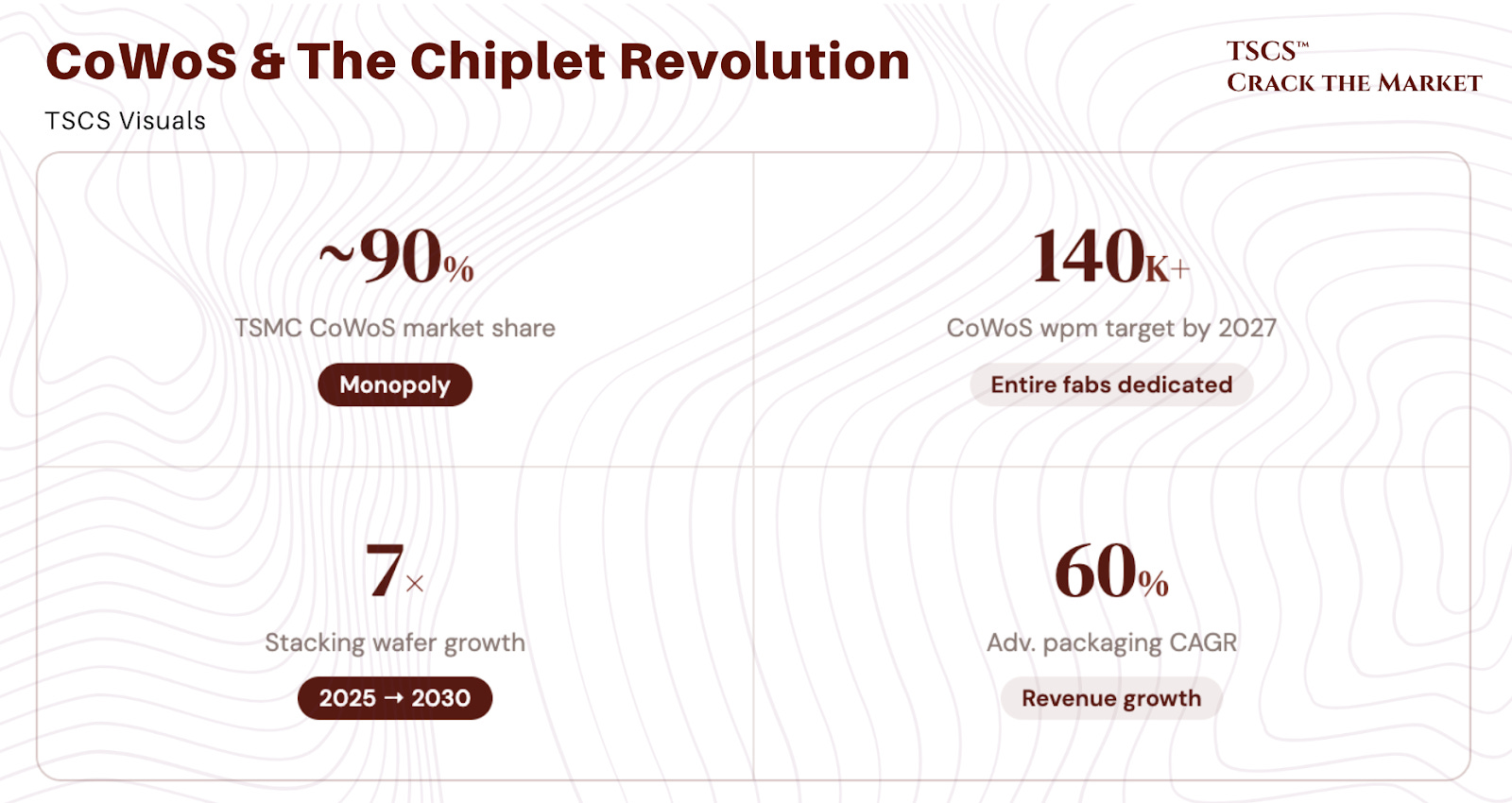
From 2D to 2.5D to 3D: the stacking roadmap
CoWoS is 2.5D: multiple dies sitting side by side on an interposer. The next step is true 3D: dies stacked directly on top of each other.
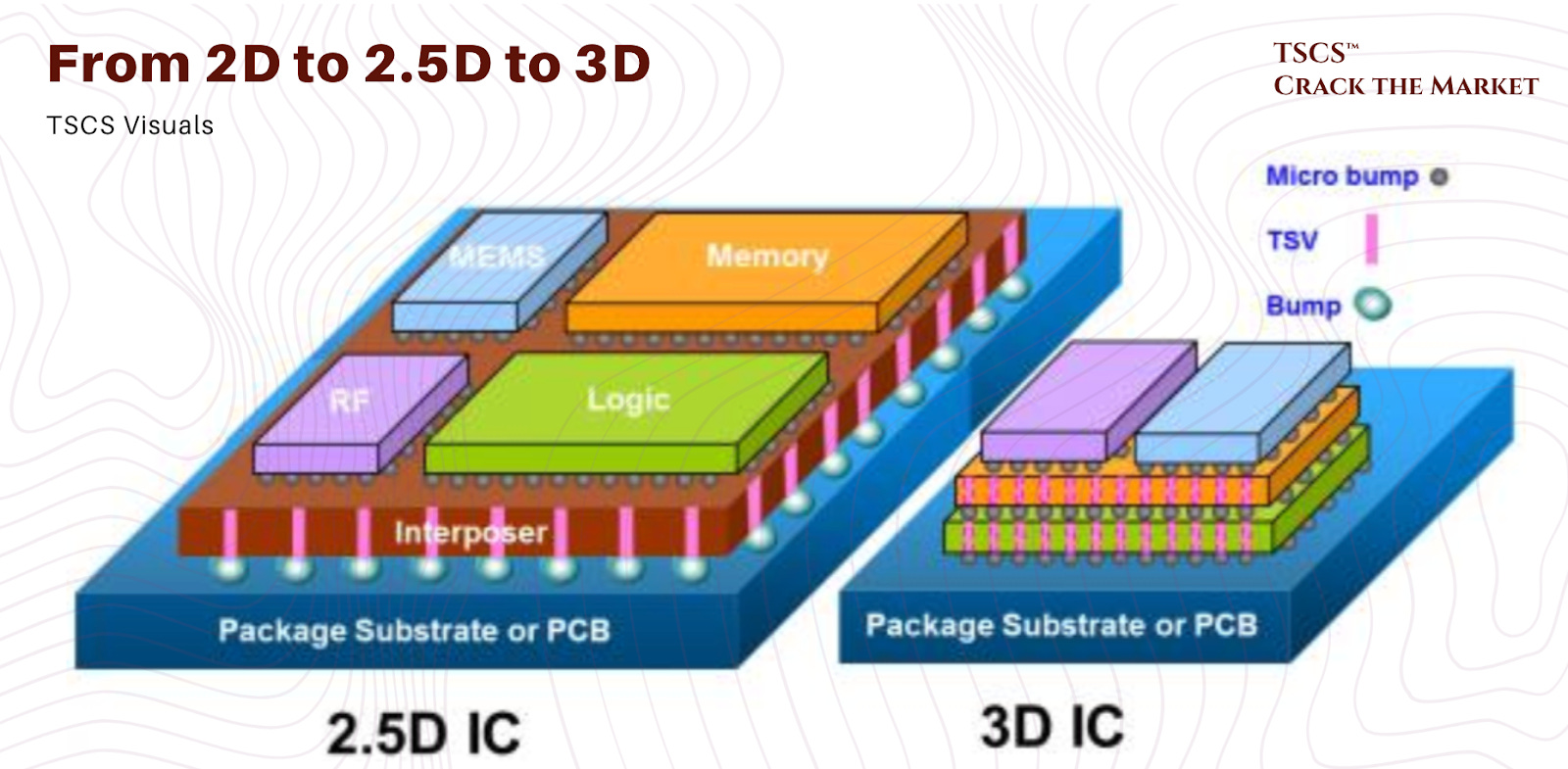
TSMC’s SoIC (System on Integrated Chips) uses hybrid bonding, where silicon and copper surfaces are polished to atomic smoothness and fused directly without solder. Copper atoms bond at the molecular level, creating ultra-dense vertical connections with minimal heat and latency. Data travels the shortest possible path: straight up and down. SoIC is still emerging in 2026 but adoption should accelerate sharply from 2027 onward as hyperscalers design custom AI silicon optimized for 3D stacking.
The stacking revolution extends well beyond logic. The biggest volume contributors by 2030 will be:
HBM (400,000 wpm today, the dominant source of stacking demand), driven by AI hyperscaler capex. Nvidia’s GPU roadmap tells the story: Hopper had 2 GPU dies and 48 HBM dies. Blackwell Ultra has 2 GPU dies and 144 HBM dies. Rubin Ultra will have 4 GPU dies and 256 HBM dies. The HBM die count per system is growing faster than the logic die count.
NAND CBA (CMOS Bonded Array) hybrid bonding, rising from over 100,000 wpm today to likely 1 million wpm by decade-end. Kioxia is leading, and Samsung’s reported licensing of YMTC’s hybrid bonding IP (discussed in the China section) validates the technology’s commercial readiness.
DRAM CBA, starting from nothing today but projected to reach over a quarter of the market by the end of the decade. This is the next frontier for Samsung and SK Hynix.
Logic stacking (CoWoS, 3D IC, WMCM for iPhones, BSPDN) will be smaller in wafer volume but enormous in value, given the ASPs of the chips being packaged.
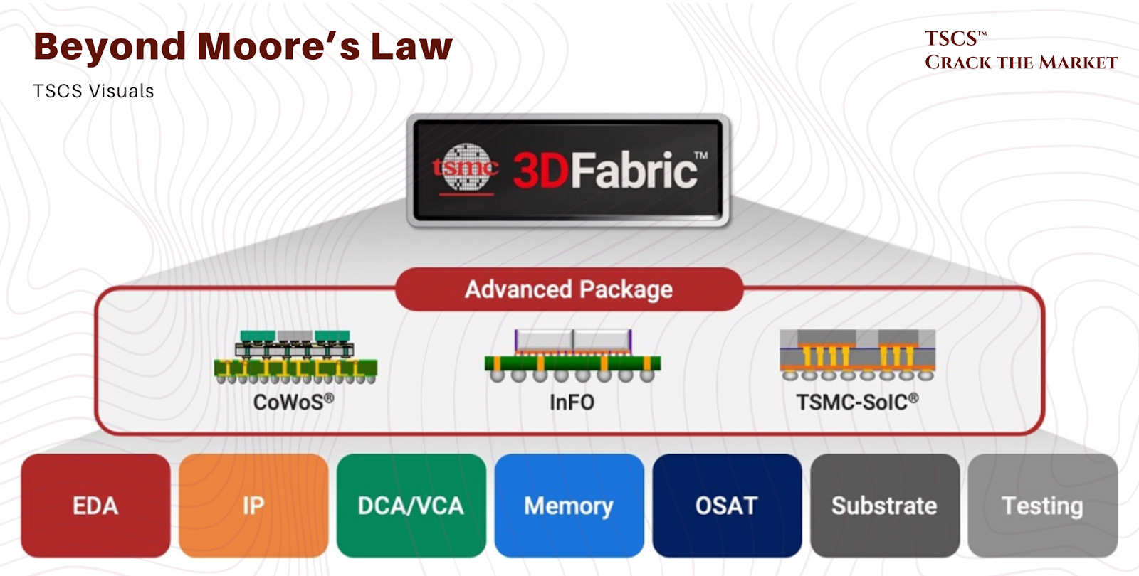
TSCS view: The stacking trajectory from 7% to 35%+ of total wafer consumption by 2030 is the kind of structural shift that creates multi-year compounding opportunities in the companies supplying the enabling equipment. Three names stand out to us. Besi has over 90% share in die-to-wafer hybrid bonding, the exact technology required for SoIC, HBM4, and NAND CBA. Disco controls 80% of precision grinding and dicing, a step that becomes more critical and more frequent as wafers are thinned for 3D stacking. Advantest holds 58% of the ATE market overall and 65% of HBM testing specifically, and testing intensity per chip is rising exponentially as multi-die packages require verification at every integration step, not just final test. These are not speculative plays on a future technology. The volume ramp is happening now, the capacity expansions are funded, and the order books are filling. The risk is not adoption. The risk is that valuations already reflect the growth, which at 30 to 45x forward earnings for some of these names, is a legitimate concern. More on this in the investor playbook.
Investor’s Strategy: how to own the semicap cycle
Semicap companies are, on paper, everything a quality-oriented investor wants: monopolistic market positions, low capex intensity, rising FCF margins, structural growth tailwinds, and customers who cannot switch. The catch is that the market has figured this out. The entire space has doubled from its April 2025 lows, and the question is no longer “are these great businesses?” but “what are you paying for greatness?”
The bull case in four sentences
Equipment intensity per node is rising structurally. Competition is frozen by antitrust and physics. AI capex is creating the most powerful demand signal since the smartphone era. FCF margins have expanded from 10% in 2013 to 20 to 30% today with no sign of reversal.
The rerate: what happened and where we are
The semicap space hit a cyclical trough in early 2025. Memory oversupply crashed DRAM and NAND capex. Fabs cut orders as post-pandemic inventories normalized. Consumer electronics demand softened. Capital rotated out of semicaps and into direct AI plays (Nvidia, hyperscalers), with the market treating equipment companies as second-derivative losers rather than AI beneficiaries.
By late 2025, the narrative inverted. Hyperscaler capex surged to record levels for 2026. TSMC’s order book for advanced nodes filled completely. A memory supercycle materialized with historic price hikes and shortages across DRAM and NAND. The market recognized, belatedly, that every AI chip begins its life in a fab equipped by these five companies.
The result: NTM P/E multiples expanded from 13 to 22x at the trough to 29 to 40x today. On a two-year forward basis (more appropriate given capex visibility), the space rerated from 12 to 20x to 25 to 32x. Rich, but still below the 2021 peaks when ASML hit 42x and ASMi reached 34x on FY2 earnings.
Our view: We want to be honest about where we think the risk-reward sits. The fundamentals are as strong as they have been in the history of this industry. Order books are full, customer capex plans have multi-year visibility, and the structural drivers (AI, reshoring, node complexity, stacking) are reinforcing rather than competing. But multiples have moved first. Further price appreciation from here is more likely to come from EPS revisions and execution than from multiple expansion. The setup is “own these through earnings beats,” not “buy the rerate.” Geopolitical newsflow (particularly around China export controls) can compress multiples 20 to 30% in weeks, as we saw repeatedly in 2023 and 2024. The correct posture is conviction on the fundamentals with discipline on entry points. If you are building a position, you want to be adding on the inevitable geopolitical-driven pullbacks, not chasing the current euphoria.
The companies: who owns what
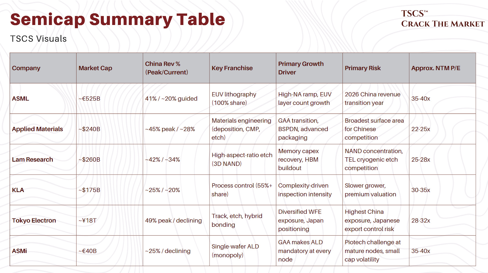
ASML ($525 billion market cap) is the cornerstone. 100% EUV monopoly, highest visibility via its backlog, and the strongest moat in the sector. The 2026 thesis is straightforward: China revenue declines from abnormal levels (41% of sales at peak) toward 20%, offset by non-China cyclical recovery and the High-NA EUV ramp. ASML trades at the highest multiple in the group because the market grants monopolists a premium, and it should. The risk is that 2026 becomes an “in-between year” where China declines faster than non-China recovers, creating a temporary earnings air pocket that the multiple may not bridge.
Our view: ASML is the one semicap stock we would hold through anything short of a global recession. The EUV franchise is impregnable, High-NA extends the runway through the 2030s, and the installed base services business provides a rising earnings floor. The China transition is real but manageable, and we suspect the market will give ASML credit for the 2027/2028 EUV ramp before the 2026 China decline fully materializes in reported numbers. ASML is the foundational position in any semicap portfolio, the one name whose moat durability justifies permanent ownership regardless of where we are in the cycle. The only caveat: it is never cheap. You pay up for ASML, and you accept that.
Applied Materials ($240 billion) is the generalist king. Broadest portfolio in the industry across deposition, etch, CMP, and process control. Uniquely positioned in materials engineering, which is precisely what the GAA transition and advanced packaging demand. Lower China risk than peers at roughly 30% of revenue. Strong services business that acts as an earnings stabilizer. Often viewed as undervalued relative to ASML and KLA, which is probably correct but has been “probably correct” for years without the gap closing.
Our view: AMAT is the best risk-adjusted entry point in the semicap space today. It has the broadest exposure to every major technology inflection (GAA, BSPDN, advanced packaging, HBM), the most diversified revenue base, and the lowest China concentration among the top five. The market persistently undervalues it relative to the specialists because “generalist” sounds boring. But when every segment of WFE is growing simultaneously (which is what a synchronized upcycle looks like), the generalist captures more of the total wallet than any specialist can. The discount to ASML and KLA on a growth-adjusted basis is, in our view, unwarranted.
Lam Research ($260 billion) is the memory beta play. Dominant in etch and deposition for 3D NAND, where high-aspect-ratio etching through 200+ layers is its franchise. The most leveraged name to a memory capex recovery, which is both the opportunity and the vulnerability. Upgrade revenue surged over 90% year-over-year in late 2025, confirming the cycle turn.
Our view: Lam is the semicap stock you own when you have conviction that the memory supercycle has legs, and we do have that conviction in the near term. HBM demand is structural. DRAM pricing is tight. NAND is finally emerging from its capex trough. But Lam carries two risks the market is underweighting. First, NAND concentration: if the NAND recovery disappoints (and NAND has disappointed before, repeatedly), Lam takes a disproportionate hit. Second, Tokyo Electron’s cryogenic etch technology is a credible competitive threat in specific process steps. We are constructive on Lam but would size it smaller than AMAT or ASML in a semicap portfolio.
KLA ($175 billion) is the quality compounder. Over 50% share in inspection and metrology, highest gross and operating margins in the group, and the most defensible moat against Chinese substitution (below 5% domestic self-sufficiency at advanced nodes). Process control intensity has risen from 5.9% to 8.6% of WFE over seven years because complexity drives inspection demand, and complexity only goes in one direction.
Our view: We discussed KLA’s moat extensively in the China section of this piece. The short version: if you want semicap exposure with the lowest China risk, the highest margins, and the most structural growth tailwind (complexity-driven inspection intensity), KLA is your answer. It trades at a premium for a reason, and the premium is justified. The only knock is that it is a slower grower than the more cyclical names, which means it underperforms in the early innings of a sharp upcycle. In a risk-adjusted, full-cycle framework, KLA is arguably the best business in the entire WFE chain.
Tokyo Electron ($120 billion) is the Japan play. Diversified across track, etch, and deposition, with a growing hybrid bonding position (32% share). Has benefited massively from Chinese demand filling gaps left by US export controls on American competitors. Strong margin expansion story and new product cycles (cryogenic etch) driving robust EPS growth.
Our view: TEL is the semicap name we have the most nuanced view on. The positives are real: diversified portfolio, margin expansion, yen tailwind, and a backend positioning (hybrid bonding) that aligns perfectly with the stacking mega-trend. But TEL peaked at 49% China revenue, the highest of any major peer, and that revenue was partially a function of regulatory arbitrage (Japanese companies face looser restrictions than US companies). If Japan tightens export controls further (which is the direction of travel), TEL’s China advantage erodes. We would not avoid TEL, but we would underweight it relative to the US and Dutch names until the China revenue normalization is complete.
ASMi ($40 billion) is the pure-play on physics. Dominant in single-wafer ALD, which becomes mandatory at 2nm/GAA. Smaller than the platform companies but growing faster because its core technology is moving from “nice to have” at FinFET nodes to “cannot fabricate without it” at GAA. The market prices it as a high-growth secular compounder, and that pricing is correct.
Our view: ASMi offers the highest expected return in the semicap space on a 3 to 5 year horizon, given that the GAA adoption curve mechanically expands its addressable market with every node transition. The GAA transition makes ALD structurally more important with every node, and ASMi’s share of WFE should expand as a mathematical consequence of where the industry is heading. The risk is Piotech’s emerging challenge at mature nodes in China, but at the leading edge (where the growth and margins live), ASMi has no credible competitor. At $40 billion market cap, it is small enough that the position can compound meaningfully. The volatility will be higher than ASML or KLA because it is a smaller, more concentrated business, but the growth rate justifies the ride.
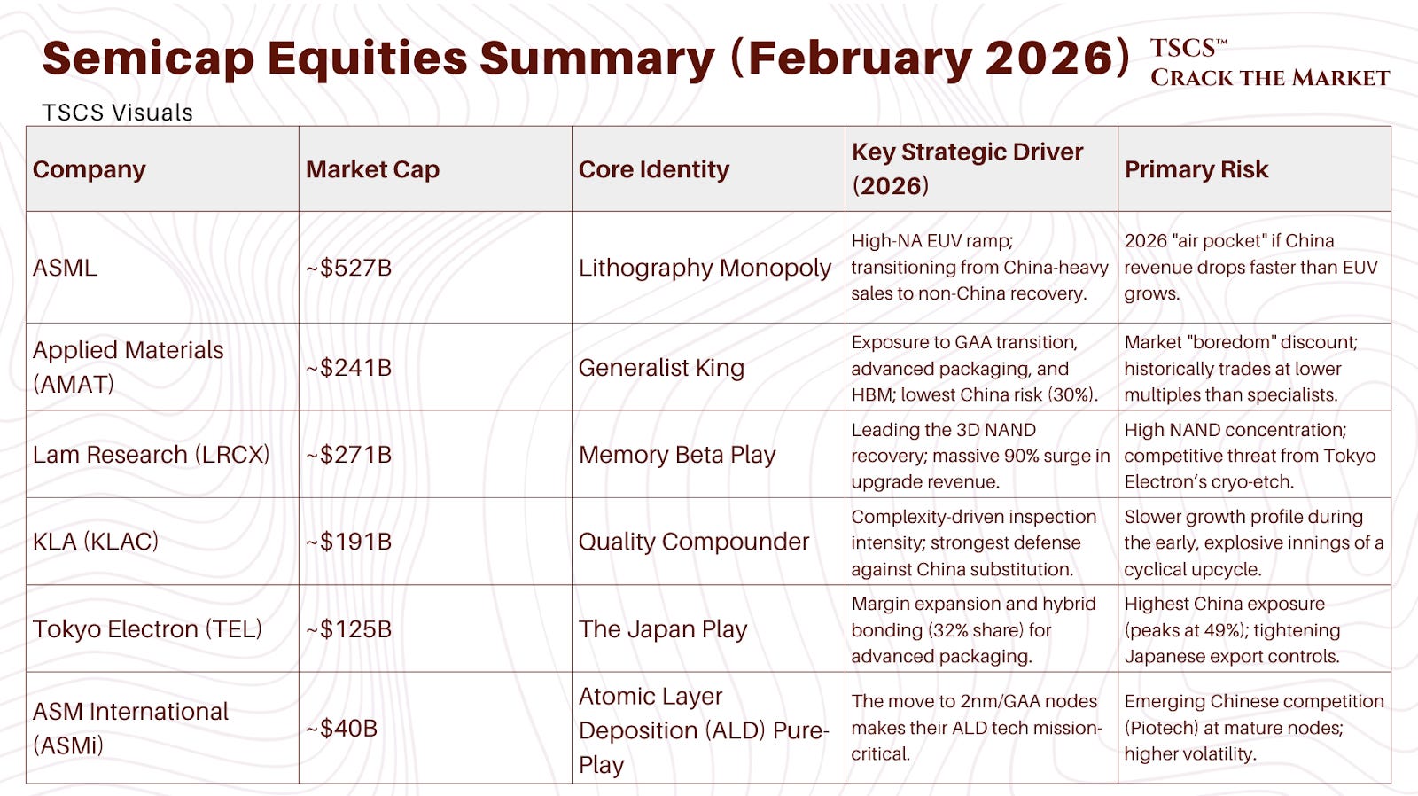
The back-end winners
Advantest ($112 billion) holds 58% of the global ATE market and 65% of HBM testing. Near-monopoly on testers for AI accelerators. Testing intensity per chip is rising exponentially because multi-die packages require verification at every integration step. The toll booth that verifies every AI chip before it ships.
Disco ($45 billion) controls 80% of precision grinding and dicing. 70% gross margins. A direct volume beneficiary of HBM capacity expansion and wafer thinning for 3D stacking. The picks-and-shovels play within the picks-and-shovels sector.
Besi ($15 billion) has over 90% share in die-to-wafer hybrid bonding. The dominant enabler of the technology that makes SoIC, HBM4, and NAND CBA possible. Premium valuation (over 60% gross margins) for a monopolistic position in a game-changing technology. The adoption inflection is expected from 2026 onward.
Teradyne ($42 billion) is the number two ATE player (35 to 39% share), strongest in mobile (Apple supply chain), analog, and mixed-signal testing. Also owns Universal Robots, giving it an unrelated but interesting call option on industrial automation. The cyclical recovery play for investors who want semicap exposure away from the crowded AI trade.
Our view: Among the back-end names, Besi is the one that excites us most on a 3 to 5 year horizon. Hybrid bonding is the enabling technology for the entire stacking roadmap, and Besi owns the equipment franchise with 90%+ share. The risk is concentration: if hybrid bonding adoption is slower than expected, or if a competitor emerges, the premium valuation compresses hard. But based on everything we see in the stacking volume projections (7% to 35%+ of wafers by 2030), the adoption curve is steepening, not flattening. Advantest is the safer way to play the same theme, given its larger market, broader customer base, and structural testing intensity tailwind from chiplet proliferation. Both are expensive. Both are probably worth it.
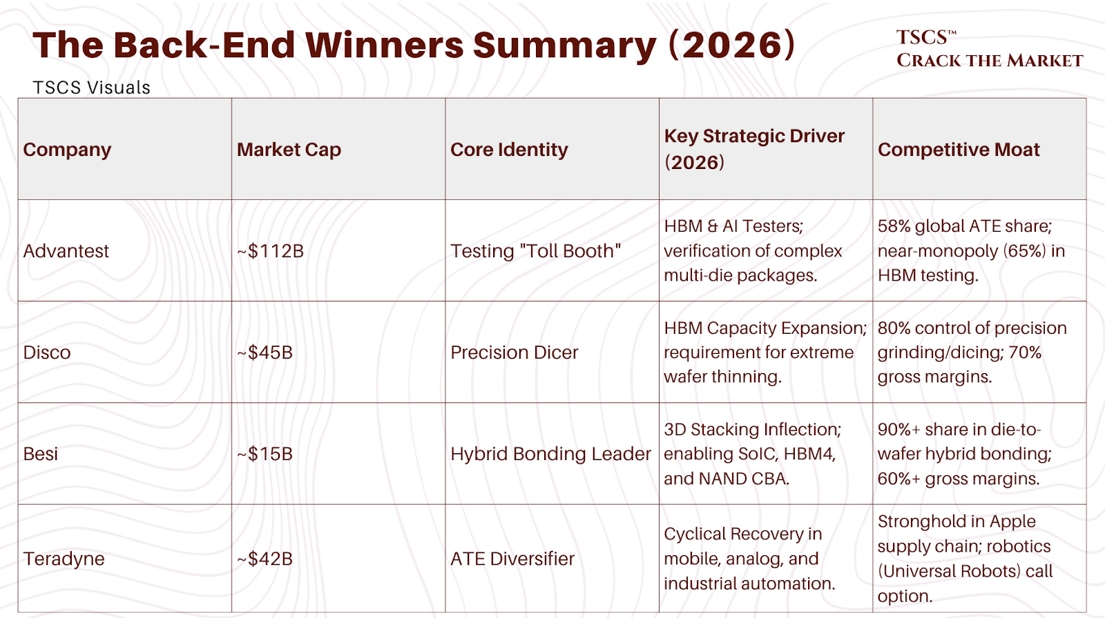
What are you actually paying for?
Semicap valuations have expanded significantly from their early 2025 trough, and discipline requires understanding what the current prices embed.
Historical context: the semicap group has traded between 12-15x NTM earnings at cyclical troughs (early 2019, early 2023, early 2025) and 38-45x at cyclical peaks (late 2021). The current range of 27-40x NTM P/E sits in the upper half of the historical band, though on a two-year forward basis (more appropriate given the visibility of TSMC’s capex plans and equipment lead times), the range compresses to 22-32x.
Relative to comparable capital goods monopolists, the valuations are not unreasonable. Danaher trades at 25-28x forward earnings with mid-single-digit organic growth. Roper Technologies trades at 28-30x with similar growth. The semicap group offers higher structural growth (9-12% versus 5-7%), higher FCF margins (25-30% versus 20-25%), and arguably deeper competitive moats (physics-based rather than distribution-based). A premium to traditional industrials is justified. The question is how much.
On a free cash flow yield basis, most semicap names yield 2.0-3.0% today versus 3.5-4.0% at their early 2023 troughs and 1.5-2.0% at the late 2021 peak. The current yield implies the market is pricing in durable growth but not euphoric growth, which feels about right given the visibility.
Our view: We think 25-30x NTM earnings is the fair value range for the group, given 9-12% structural growth, 25-30% FCF margins, monopoly positioning, and the installed base revenue floor that limits downside cyclicality. At current prices, most names trade at the upper end of fair value: not overvalued, but not offering a meaningful margin of safety. The risk-reward improves materially on any 15-20% pullback, which geopolitical catalysts have delivered repeatedly (ASML declined roughly 35% from its July 2024 peak to its April 2025 trough on export control fears, then recovered fully within six months). The posture we recommend is to own these businesses through the cycle, add on policy-driven drawdowns, and resist the temptation to chase after 20%+ rallies. The structural case is a five-year thesis. The entry point matters on a one-year view.
Risks worth actually worrying about
Geopolitics is number one. If the US bans all equipment exports to China, including mature-node tools, that is a $15 to 25 billion revenue hole across the industry. China still represents a quarter to a third of sales for most semicap companies. The Busan agreement was a tactical pause, not a structural resolution.
AI sentiment reversal is number two. Semicap stocks have increasingly correlated with the AI trade. If hyperscaler capex disappoints, or if the market decides AI infrastructure spending has peaked (even temporarily), semicap multiples will compress faster than earnings estimates can adjust.
The macro is number three. A deep recession that crushes consumer demand for phones, PCs, and cars would eventually flow through the entire chain. Equipment companies sit at the end of a long bullwhip, and the whip can crack in both directions.
Customer consolidation is number four. The entire semicap thesis rests on rising cost per node, but there is an implicit assumption that customers will always pay. Intel Foundry is hemorrhaging cash partly because it cannot earn adequate returns on the equipment investment required for leading-edge nodes; its foundry division reported cumulative operating losses exceeding $16 billion over 2023-2025.
Samsung’s foundry division is loss-making at advanced nodes with disastrous 3nm yields. If the cost curve steepens further at A16 and beyond, we could see the buyer base for leading-edge equipment consolidate from three (TSMC, Samsung, Intel) to effectively one. A monopsony scenario, where TSMC holds 80%+ of leading-edge foundry volume, would shift bargaining power toward the buyer, even against monopolist equipment suppliers. TSMC could, in theory, begin extracting pricing concessions that the current oligopoly structure does not permit.
Cyclical reassertion is number five. Structural growth does not eliminate cyclicality; it raises the floor while the amplitude persists. WFE experienced peak-to-trough declines of roughly 30% in 2019 and 20-25% in 2023, even within a secular uptrend. The current setup (synchronized strength across logic, memory, packaging, and reshoring) feels like it has duration, but the semiconductor industry has a long history of rewarding consensus optimism with inventory corrections. The most plausible near-term trigger for a WFE downturn would be a combination of NAND oversupply (YMTC and domestic Chinese expansion flooding commodity flash), a pause in hyperscaler ordering (even a one-quarter delay in GPU server installations would ripple through the chain), and geopolitical shock (a new round of export controls more severe than December 2024). None of these alone would break the structural thesis, but in combination they could produce a 15-25% WFE correction that temporarily compresses semicap earnings and multiples. The correct response is not to avoid the sector but to maintain liquidity to add on such corrections. Every semicap investor should know in advance what price they want to pay, so that when the drawdown arrives, they are buyers rather than panickers.
We think this risk is low in the near term: TSMC needs equipment companies as much as they need TSMC, lead times of 18-24 months for EUV systems give equipment makers structural leverage, and Samsung and Intel both have stated commitments to advanced node investment that make full exit unlikely before 2028. But it is the correct long-term bear case for the sector that almost nobody discusses, and investors pricing semicap stocks at 35x forward earnings should at least be aware of it.
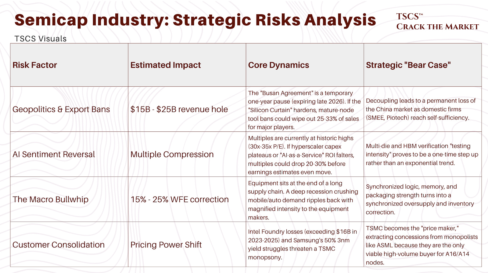
Capital allocation: what these companies do with the cash
The semicap oligopoly generates enormous free cash flow, and how it is deployed matters for long-term returns. In aggregate, the top six Western equipment companies (ASML, AMAT, Lam, TEL, KLA, ASMi) produce roughly $35-40 billion in annual FCF and growing.
R&D reinvestment is the first priority and the foundation of the moats. ASML spent €4.7 billion on R&D in 2025, approximately 14% of revenue, funding High-NA EUV development and the early stages of hyper-NA. KLA reinvests 14-15% of revenue. AMAT increased R&D spending 10% in FY2025 to secure positioning at GAA and BSPDN nodes. Lam spent $2.1 billion (11.4% of revenue). These R&D rates are high relative to industrial peers but necessary: the semicap oligopoly is ultimately a knowledge business, and the moats decay without continuous reinvestment.
Capital returns to shareholders are the second priority, and they are substantial. ASML returned €3.0 billion to shareholders in 2024 through dividends and buybacks, completing a €7.6 billion buyback program in December 2025 and announcing a new program alongside a 4.9% dividend increase. KLA returned $3.0 billion in its fiscal 2025 (ended June), including $2.15 billion in buybacks and $905 million in dividends, with a 15% dividend CAGR since 2006 and a 12% dividend increase announced for fiscal 2026. Lam repurchased $3.4 billion of stock in FY2025 and paid $1.15 billion in dividends, funded by $6.2 billion in operating cash flow. AMAT runs aggressive buybacks at 3-4% of shares annually, with its AGS services income alone covering the entire dividend.
M&A is effectively off the table for the large players. Applied Materials’ attempted merger with Tokyo Electron was blocked in 2015. Lam’s $10.6 billion bid for KLA was terminated in 2016 amid antitrust concerns. The regulatory environment has not loosened. This means that FCF growth translates almost entirely into either R&D reinvestment or shareholder returns, and FCF per share growth will continue to outpace FCF growth as buybacks compound. For a sector growing revenue at 9-12% annually with 25-30% FCF margins and 2-4% annual share count reduction, the EPS growth algorithm is structurally attractive even if multiples stay flat.
Our view: The risk we think the market is most underpricing is the geopolitical one. Not because we expect a full China ban (we do not, at least not imminently), but because the optionality of escalation sits entirely with Washington and the semiconductor companies have no ability to hedge it. A single regulatory announcement can erase 15 to 20% of market cap in a session, as we saw multiple times in 2023 and 2024. The correct portfolio response is not to avoid semicaps (the structural case is too strong) but to size positions with the understanding that geopolitical vol is a feature of this sector, not a bug. Keep dry powder for the inevitable policy-driven drawdowns. They are buying opportunities dressed as crises.
Disclaimer: This is not financial advice. TSCS provides research and analysis for informational and educational purposes only. Always conduct your own due diligence before making investment decisions. Positions may be held in securities discussed.
 | A guest post by
|
I have a very small part in the etch side of the business. Familiar with all these companies and “strategies”. This is the most honest and in depth article I’ve ever seen. Good job my man, anyone who see this, pour your money into all of them